
Ablative scribing of solar cell structures

Inactive Publication Date: 2011-11-01
BEIJING APOLLO DING RONG SOLAR TECH
View PDF5 Cites 21 Cited by
  • Summary
  • Abstract
  • Description
  • Claims
  • Application Information

AI Technical Summary

Benefits of technology

[0009]Another aspect of the invention relates to a method of forming monolithically integrated photovoltaic cells involving providing a substrate having a plurality of layers of a thin film photovoltaic stack deposited thereon, including a top layer and an underlayer; focus

Problems solved by technology

For example, in certain embodiments, pulse widths in between and exclusive of nanoseconds and femtoseconds are used, nanoseconds being too long to achieve the requisite peak intensity and femtoseconds too short, resulting in non-linear absorption.

Method used


Image

  • Ablative scribing of solar cell structures
  • Ablative scribing of solar cell structures
  • Ablative scribing of solar cell structures

Examples


Embodiment Construction

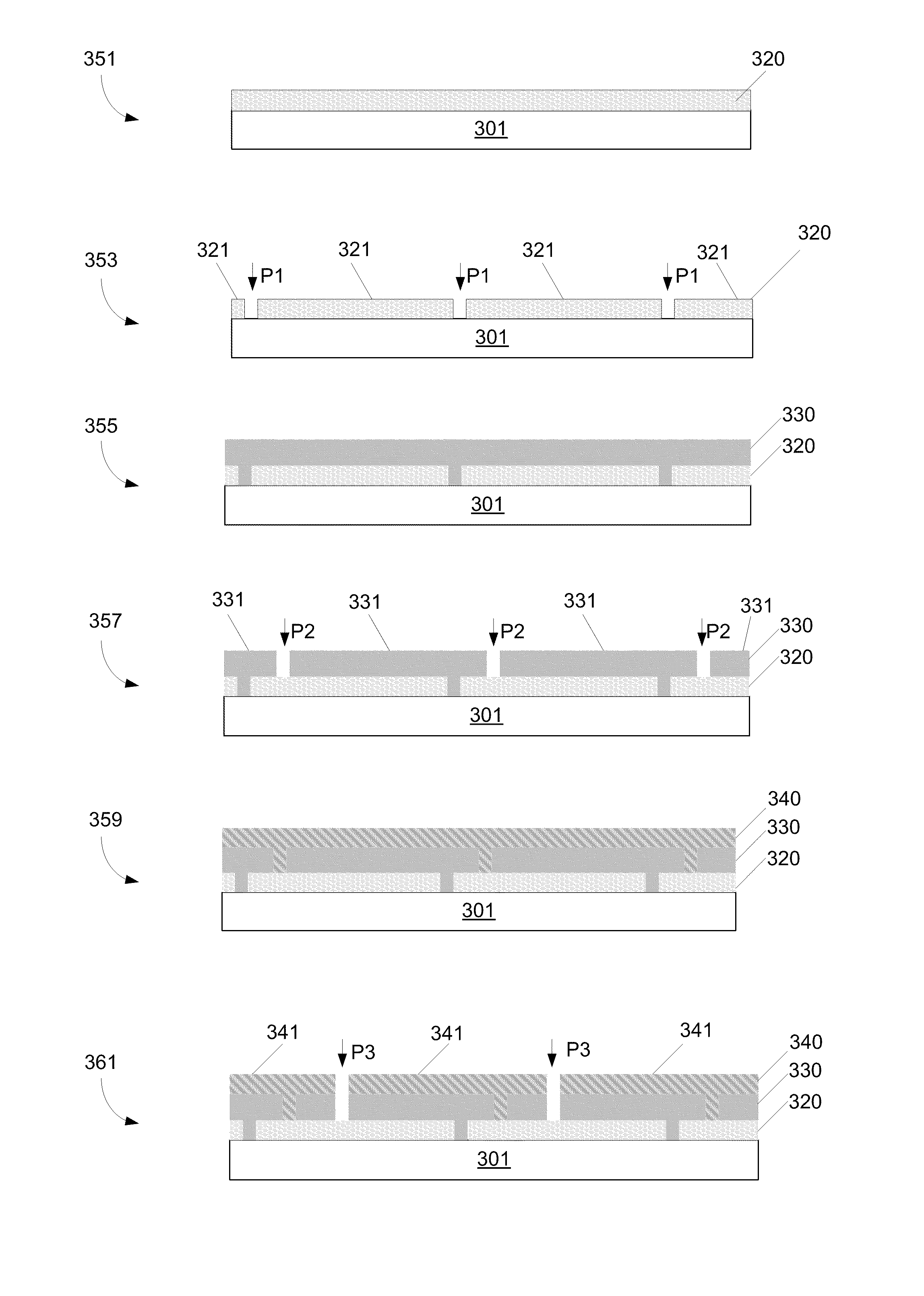
[0020]Reference will now be made in detail to specific embodiments of the invention. Examples of the specific embodiments are illustrated in the accompanying drawings. While the invention will be described in conjunction with these specific embodiments, it will be understood that it is not intended to limit the invention to such specific embodiments. On the contrary, it is intended to cover alternatives, modifications, and equivalents as may be included within the spirit and scope of the invention. In the following description, numerous specific details are set forth in order to provide a thorough understanding of the present invention. The present invention may be practiced without some or all of these specific details. In other instances, well known mechanical apparatuses and / or process operations have not been described in detail in order not to unnecessarily obscure the present invention.

[0021]Provided herein are methods for laser scribing layers of thin film photovoltaic stacks...


PUM


Abstract

Provided herein are improved methods of laser scribing photovoltaic structures to form monolithically integrated photovoltaic modules. The methods involve forming P1, P2 or P3 scribes by an ablative scribing mechanism having low melting, and in certain embodiments, substantially no melting. In certain embodiments, the methods involve generating an ablation shockwave at an interface of the film to be removed and the underlying layer. The film is then removed by mechanical shock. According to various embodiments, the ablation shockwave is generated by using a laser beam having a wavelength providing an optical penetration depth on the order of the film thickness and a minimum threshold intensity. In one embodiment, material including an absorber layer is scribed using an infrared laser source and a picosecond pulse width.

Description

BACKGROUND OF THE INVENTION[0001]Photovoltaic cells are widely used for generation of electricity, with multiple photovoltaic cells interconnected in module assemblies. Such modules may in turn be arranged in arrays and integrated into building structures or otherwise assembled to for large scale conversion of solar energy into electricity by the photovoltaic effect.[0002]Certain photovoltaic cell fabrication processes involve monolithic integration of the cells of a module. For thin film solar modules, this involves depositing thin film materials on a substrate to form a light absorbing layer sandwiched between electrical contact layers. The front or top contact is a transparent and conductive layer for current collection and light enhancement, the light absorbing layer is a semiconductor material, and the back contact is a conductive layer to provide electrical current. In one example of a fabrication process, a metallic back electrical contact layer is deposited on a substrate. A...

Claims


Application Information

Patent Timeline
IPC IPC(8): H01L21/00
CPCH01L31/0465H01L31/0463Y02E10/50
Inventor GHANDOUR, OSMANAUSTIN, ALEXLEE, DAEBONGCORNEILLE, JASON STEPHENTEIXEIRA, JAMES
Owner BEIJING APOLLO DING RONG SOLAR TECH
Learn More