Electron beam writing method, fine pattern writing system, method for manufacturing uneven pattern carrying substrate, and method for manufacturing magnetic disk medium

a writing system and pattern technology, applied in the field of fine pattern writing system, can solve the problems of backward scattering, insufficient dose, affecting the forming accuracy of a desired pattern, etc., and achieve the effect of high accuracy, easy manufacturing, and excellent properties

Inactive Publication Date: 2011-11-01
FUJIFILM CORP
View PDF5 Cites 7 Cited by
  • Summary
  • Abstract
  • Description
  • Claims
  • Application Information

AI Technical Summary

Benefits of technology

[0023]Further, when the elements are written by microscopically vibrating the electron beam back and forth in a circumferential direction of the substrate and deflecting the electron beam in a radial direction orthogonal to the vibration direction, the proximity-effect correction for an element in the densely arranged region having the same shape as that of an element in the sparsely arranged region is performed such that the element is written by reducing the writing-ON-time and increasing the deflection speed in the radial direction by an amount corresponding to the reduced amount of the writing-ON-time, thereby reduction correcting the amount of dose.
[0036]According to the second method for manufacturing a disk medium of the present invention, a magnetic disk medium is manufactured using a magnetic transfer master substrate obtained through the steps of exposing a desired fine pattern on a substrate applied with a resist by the electron beam writing method described above and forming thereon an uneven pattern corresponding to the desired fine pattern to magnetically transfer a magnetic pattern corresponding to the uneven pattern formed on the surface of the master substrate to the magnetic disk medium. In the case of the magnetic transfer master substrate, the substrate has thereon a fine pattern of a magnetic layer, so that a magnetic recording medium having excellent properties may be manufactured easily by bringing the master substrate into contact with the magnetic recording medium and applying a magnetic field thereto using magnetic transfer technology, and transfer forming a magnetic pattern corresponding to the pattern of the magnetic layer of the master substrate on the magnetic recording medium.

Problems solved by technology

Further, the beam incident on the substrate is scattered, causing backward scattering in which the beam is bounced back from the bottom of the substrate with a large scattering angle.
On the other hand, in a sparsely arranged region where only a few elements to be written are arranged around as in a contour portion of the aggregation of element arrangement, the number of impacting scattered electrons is small and the proximity effect becomes small, so that the amount of dose tends to be insufficient.
If the amount of dose varies according to the element density, when a resist after writing exposure is developed, the exposed resist area to be removed differs from the writing area, whereby an error occurs in the element shape, influencing the forming accuracy of a desired pattern.
The proximity-effect correction in actual electron beam writing has a problem that the setting and write control is complicated.
Fine adjustment of the amplitude for the writing of each element involves changes in the oscillation signal and control difficulties.

Method used


Image

  • Electron beam writing method, fine pattern writing system, method for manufacturing uneven pattern carrying substrate, and method for manufacturing magnetic disk medium
  • Electron beam writing method, fine pattern writing system, method for manufacturing uneven pattern carrying substrate, and method for manufacturing magnetic disk medium
  • Electron beam writing method, fine pattern writing system, method for manufacturing uneven pattern carrying substrate, and method for manufacturing magnetic disk medium

Examples


Embodiment Construction

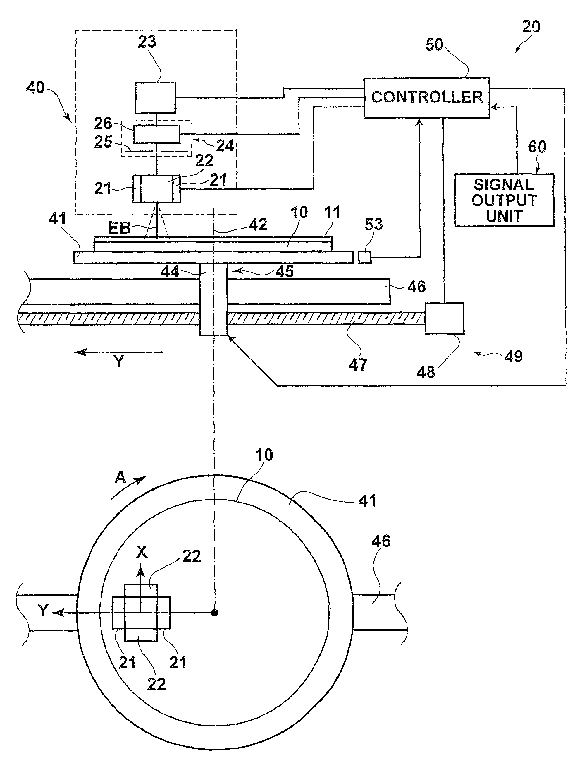
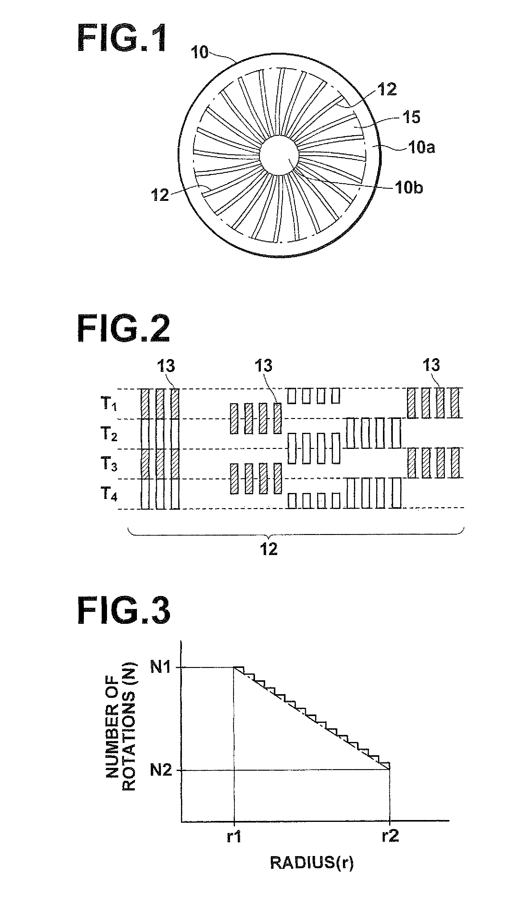
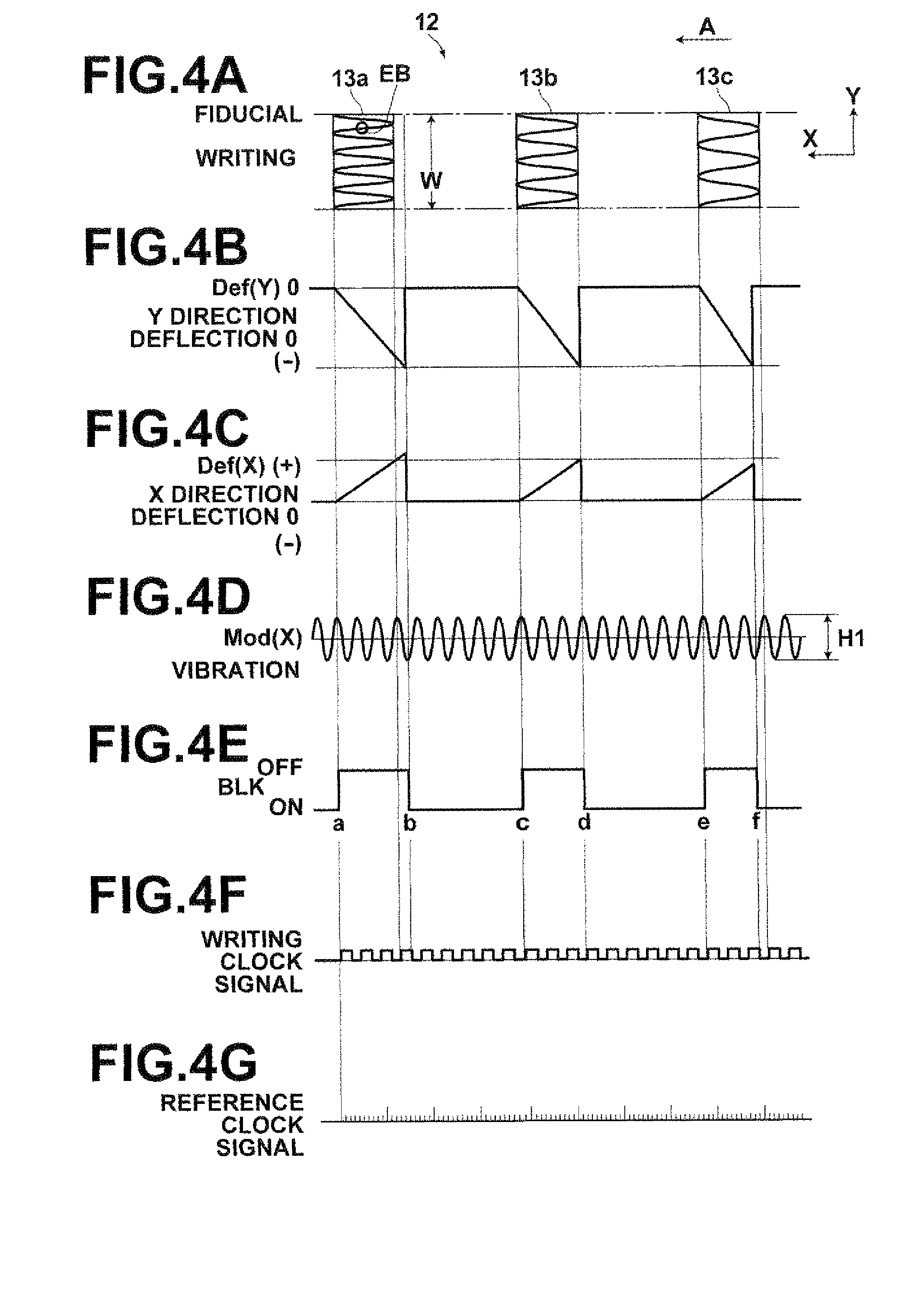
[0049]Hereinafter, exemplary embodiments of the present invention will be described in detail with reference to the accompanying drawings. FIG. 1 illustrates an example fine pattern in plan view to be written on a substrate by an electron beam writing method of the present invention. FIG. 2 is a partially enlarged view of the fine pattern. FIG. 3 is a graph illustrating the relationship between the radius of the writing position and rotational speed of a substrate. FIG. 4A is an enlarged schematic view illustrating a first writing mode which includes correction of proximity effects of fine pattern elements, and FIGS. 4B to 4G illustrate various signals, including a deflection signal and the like, used in the first writing mode shown in FIG. 4A. FIG. 5A is an enlarged schematic view illustrating a second writing mode which includes correction of proximity effects of fine pattern elements, and FIGS. 5B to 5G illustrate various signals, including a deflection signal and the like, used ...


PUM

PropertyMeasurementUnit
diameteraaaaaaaaaa
shapesaaaaaaaaaa
densityaaaaaaaaaa

Abstract

When writing the shapes of elements of a fine pattern on a substrate by microscopically vibrating the electron beam back and forth in a radial direction of the substrate or in a direction orthogonal to the radial direction and deflecting the electron beam in a direction orthogonal to the vibration direction to scan the electron beam so as to completely fill the shapes of the elements, a proximity-effect correction is performed according to the arrangement density of the elements in which the amount of dose is adjusted by setting the deflection speed faster for the writing of an element in a densely arranged region than for the writing of an identical element in a sparsely arranged region.

Description

BACKGROUND OF THE INVENTION[0001]1. Field of the Invention[0002]The present invention relates to an electron beam writing method and a fine pattern writing system for writing a fine pattern according to a desired uneven pattern when manufacturing an imprint mold, magnetic transfer master substrate, or the like for a high density magnetic recording medium, such as a discrete track medium, bit pattern medium, or the like.[0003]The invention also relates to a method for manufacturing an uneven pattern carrying substrate, including an imprint mold, magnetic transfer master substrate or the like, having an uneven pattern surface formed through a writing step performed by the electron beam writing method described above. The invention further relates to a method for manufacturing a magnetic disk medium having an uneven pattern transferred thereto from the uneven pattern carrying substrate or imprint mold, and a method for manufacturing a magnetic disk medium having a magnetized pattern tr...

Claims


Application Information

Patent Timeline
Patent Type & Authority Patents(United States)
IPC IPC(8): G03C5/00G01Q10/04
CPCB82Y10/00B82Y40/00G11B5/59638G11B5/743G11B5/855G11B5/865H01J37/3174
Inventor KOMATSU, KAZUNORIUSA, TOSHIHIRO
Owner FUJIFILM CORP
Why Eureka
Try Eureka