Display device and electronic apparatus using the same

a technology of electronic equipment and display device, which is applied in the field of display device, can solve the problems of reducing reliability as a mobile device, increasing the size and weight of the device, and unable to accurately perform luminance control

Active Publication Date: 2011-12-06
HANNSTAR DISPLAY CORPORATION
View PDF18 Cites 11 Cited by
  • Summary
  • Abstract
  • Description
  • Claims
  • Application Information

AI Technical Summary

Benefits of technology

[0023]According to the present invention, in a display device wherein a light-detecting element is provided and a light control operation is performed according to external light, a structure where the influence of noise can be minimized and it is not necessary to provide a new circuit outside of a substrate can be obtained. This can be achieved by employing the structure where the output of an optical sensor is converted into digital data, which is resistant to noise, before being transmitted to an existing luminance control circuit, or the structure where the luminance control is completed on the substrate.

Problems solved by technology

However, even with the technologies described in the above-mentioned Patent Document, the following problems still remain.
The very small detecting current from the optical sensor flows in the wiring line and if external noise enters the cable, the luminance control will not be able to be performed accurately because the photodetecting current will not be transferred to the control circuit accurately.
The same problem occurs in the case where the output of the optical sensor is outputted as a voltage.
Concerning the effort to improve the energy-saving abilities of these devices, the power consumption of the backlight and frontlight of an LCD is a big part of the problem.
However, as explained above, while the energy-saving issue has been dealt with by some of the conventional technologies, the problems such as the increases in size and weight of the device, and the decrease in reliability as a mobile device, due to the fact that more connection lines are needed between the display device and outside, remain unsolved.

Method used


Image

  • Display device and electronic apparatus using the same
  • Display device and electronic apparatus using the same
  • Display device and electronic apparatus using the same

Examples


embodiment 1

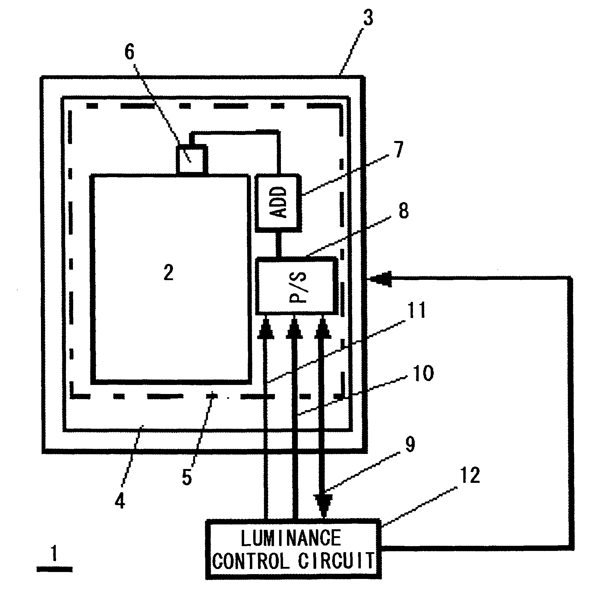
[0034]Next, a first preferred embodiment in which the present invention is applied to a transmission-type LCD with a backlight using an LED (Light Emitting Diode) will be described. The display device 1 relating to the present embodiment comprises an optical sensor 6, analog-to-digital converter circuit (ADC hereinafter) 7, and a serial-parallel converter circuit 8 provided on a substrate 4 on which a TFT driving pixels is provided, converts an output signal of the sensor 6 into a digital signal, and enables the digital signal converted into serial data to be transmitted to use it for the luminance control of the display device, corresponding to external chip-select signals.

[0035]FIG. 1 is an outline drawing of the display device relating to the first embodiment of the present invention. In reference to FIG. 1, the display device 1 comprises a backlight 3, which is the light source, the TFT substrate 4, on which the pixels (electrodes) and the TFT driving liquid crystal are provided...

embodiment 2

[0051]Next, a second embodiment in which the present invention is applied to a transmission-type LCD, as in the first embodiment, will be described. FIG. 4 is an outline drawing of the display device relating to the second embodiment of the present invention. In reference to FIG. 4, the display device 1 comprises a backlight 3, a TFT substrate 4, on which pixels (electrodes) and a TFT driving liquid crystal are provided, and a counter substrate 5 disposed so that a liquid crystal layer, not shown in the drawing, is interposed between the TFT substrate 4 and the counter substrate 5, and a display region 2 is provided.

[0052]On the TFT substrate 4, an optical sensor 6 using a photodiode is formed using the means described in Japanese Patent Kokai Publication No. JP-A-06-11690 or the like. Similarly, a luminance control circuit 15 that controls the luminance of the backlight 3 based on a signal from the optical sensor 6 is formed on the top of the TFT substrate 4. Here, the optical sens...

embodiment 3

[0059]Next, a third embodiment in which the present invention is applied to a transmission-type LCD, as in the first and second embodiments, will be described. FIG. 7 is an oblique perspective drawing showing the outline structure of the display device relating to the third embodiment of the present invention. In reference to FIG. 7, the display device 1 comprises a backlight 3, a TFT substrate 4, on which pixels (electrodes) and a TFT driving liquid crystal are provided, a counter substrate 5 disposed so that a liquid crystal layer, not shown in the drawing, is interposed between the TFT substrate 4 and the counter substrate 5, and a luminance control circuit 24, and a display region 2 is provided.

[0060]On the TFT substrate 4, an optical sensor 6 using a photodiode and a thin film wiring 19 are formed using the means described in Japanese Patent Kokai Publication No. JP-A-06-11690 or the like. Similarly, utilizing the COG (chip-on-glass) process, an IC 20 that includes an ADC and P...


PUM


Abstract

A light-detecting element, an analog-to-digital converter circuit, and a parallel-serial converter circuit are mounted on a substrate, using a thin film transistor, of an active matrix-type display device, and when a circuit is selected by an external chip-select signal, the luminance is adjusted by transmitting a signal of the light-detecting element, converted into digital data, to a luminance control circuit in sync with a clock signal.

Description

FIELD OF THE INVENTION[0001]The present invention relates to a display device and especially to a display device that can adjust the luminance according to the ambient illuminance.BACKGROUND OF THE INVENTION[0002]Recently, Liquid Crystal Display (LCD hereinafter) that has the characteristics of being thin and high definition, and Electro Luminescent Display (ELD hereinafter) that uses organic electro-luminescence element have been widely used. The former, the LCD generally has a lighting device called backlight or frontlight, and displays a picture by transmitting or reflecting the light from these light. In order to keep the display screen of such a device easy to see or power consumption low, the idea of automatically adjusting the light quantity of backlight and frontlight according to the ambient brightness has been suggested.[0003]FIG. 9 is a block diagram showing the function structure of an LCD described in Patent Document 1. In FIG. 9, 100 is an optical sensor that detects t...

Claims


Application Information

Patent Timeline
Patent Type & Authority Patents(United States)
IPC IPC(8): G06F3/038
CPCG09G3/3406G09G3/3648G09G2300/0408G09G2320/0626G09G2320/0646G09G2330/022G09G2360/144G09G2360/145
Inventor IKEDA, NAOYASUHAGA, HIROSHIOTOSE, TOMOHIKOUCHIKAWA, TATSUYASUZUKI, DAISUKE
Owner HANNSTAR DISPLAY CORPORATION
Why Eureka
Try Eureka