Organic light emitting display and method of manufacturing the same

a light-emitting display and organic technology, applied in the direction of identification means, instruments, radiation control devices, etc., can solve the problems of low luminance of emitted light and worsening the contrast of organic light-emitting displays, and achieve the effect of enhancing the light-emitting efficiency of photodiodes

Active Publication Date: 2011-12-13
SAMSUNG DISPLAY CO LTD
View PDF53 Cites 3 Cited by
  • Summary
  • Abstract
  • Description
  • Claims
  • Application Information

AI Technical Summary

Benefits of technology

[0009]Aspects of the present invention also provide an organic light emitting display capable of enhancing the light receiving efficiency of a photodiode, and a method of manufacturing the same.

Problems solved by technology

However, the organic light emitting display has a problem that, since the organic thin film layer emitting the light is made of organic materials, characteristics of the organic materials deteriorate with time, which leads to a low luminance of the emitted light.
Also, the contrast of the organic light emitting display is worsened by the reflection of light incident from the outside.

Method used


Image

  • Organic light emitting display and method of manufacturing the same
  • Organic light emitting display and method of manufacturing the same
  • Organic light emitting display and method of manufacturing the same

Examples


Embodiment Construction

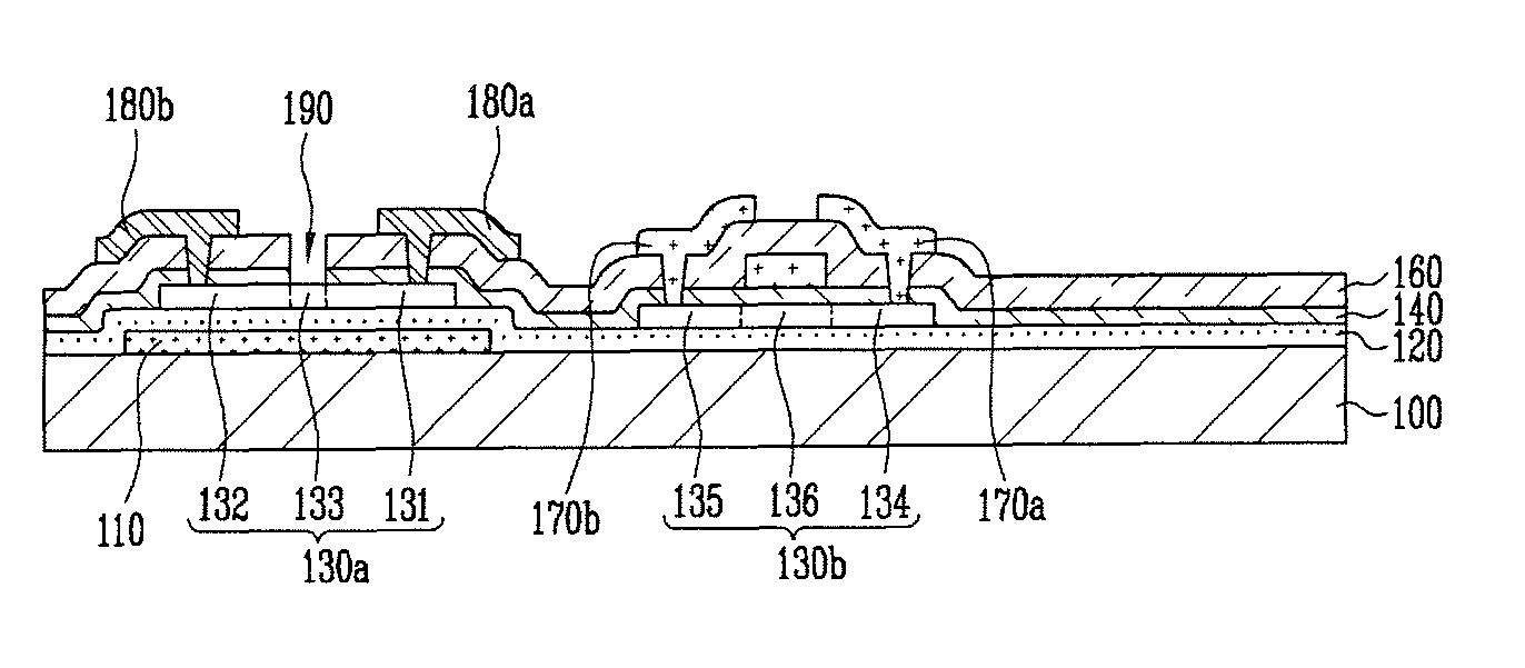
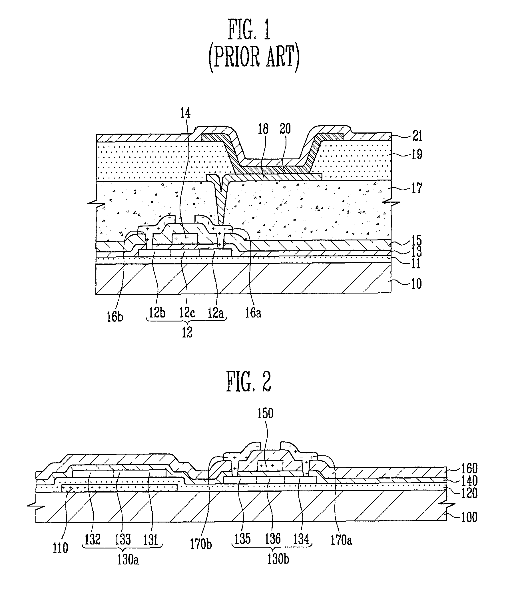
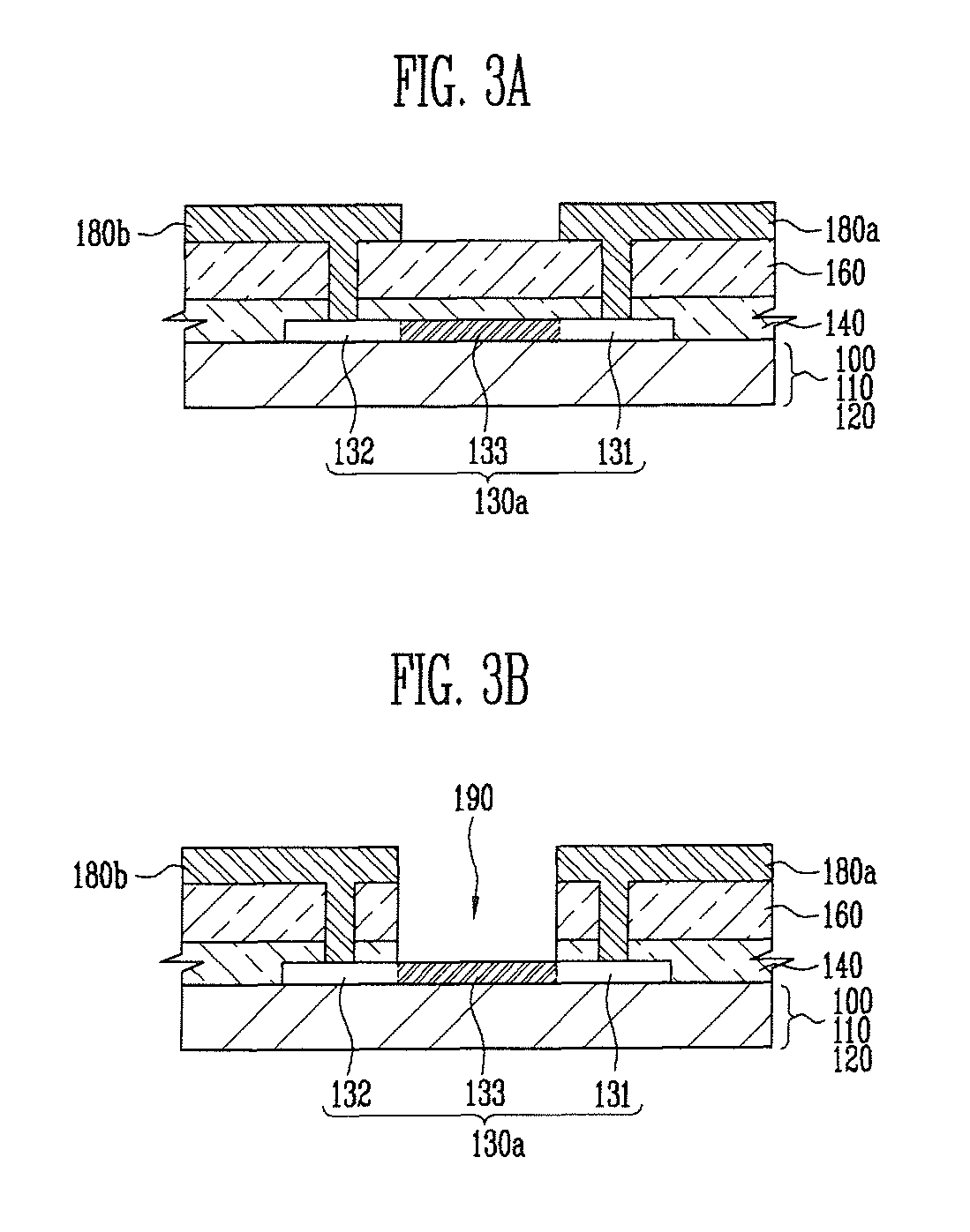
[0022]Reference will now be made in detail to the present embodiments of the present invention, examples of which are illustrated in the accompanying drawings, wherein like reference numerals refer to the like elements throughout. The embodiments are described below in order to explain the present invention by referring to the figures.

[0023]Aspects of the present invention will now be described more fully hereinafter with reference to the accompanying drawings, in which exemplary embodiments of the invention are illustrated. The invention may, however, be embodied in different forms and should not be construed as limited to the embodiments set forth herein. Rather, these embodiments are provided so that this disclosure will be thorough and complete, and will fully convey the scope of the invention to those skilled in the art.

[0024]In the figures, the dimensions of layers and regions may be exaggerated for clarity of illustration. It will also be understood that when a layer or an el...


PUM


Abstract

An organic light emitting display includes an organic light emitting diode formed on a substrate, coupled to a transistor; a photodiode formed on the substrate and including a semiconductor layer including a high-concentration P doping region, an intrinsic region with defects and a high-concentration N doping region; and a controller that uniformly controls the luminance of light emitted from the organic light emitting diode by controlling a voltage applied to the first electrode and the second electrode according to the voltage outputted from the photodiode.

Description

CROSS-REFERENCE TO RELATED APPLICATIONS[0001]This application claims the benefit of Korean Application No. 2007-93629 filed on Sep. 14, 2007 in the Korean Intellectual Property Office, the disclosure of which is incorporated herein by reference.BACKGROUND OF THE INVENTION[0002]1. Field of the Invention[0003]Aspects of the present invention relate to an organic light emitting display and a method of manufacturing the same. More particularly, aspects of the present invention relate to an organic light emitting display including a photodiode including a light receiver in which a defect site is formed by subjecting the light receiver to a dry etching process, and a method of manufacturing the same.[0004]2. Description of the Related Art[0005]An organic light emitting display is a next-generation display device having a self-light emitting characteristic. The organic light emitting display has excellent physical properties in terms of viewing angle, contrast, response time and power cons...

Claims


Application Information

Patent Timeline
Patent Type & Authority Patents(United States)
IPC IPC(8): H01L29/08H01L35/24H01L51/00G09F9/00G09F9/30H01L27/15H01L27/32H01L51/50H05B33/10
CPCH01L27/3269H01L51/56H10K59/13H10K71/00H01L33/14H01L2924/12043H10K71/30H10K50/00
Inventor KANG, CHUL-KYUPARK, BYOUNG-KEON
Owner SAMSUNG DISPLAY CO LTD
Why Eureka
Try Eureka