E-beam defect review system

a defect review and beam technology, applied in the field of beam defect review system, can solve the problems of affecting image quality, affecting the yield of a great degree, and affecting the accuracy of image enhancement, so as to save operation time and memory, enhance processing speed, and improve aberration.

Active Publication Date: 2012-01-10
ASML NETHERLANDS BV
View PDF69 Cites 11 Cited by
  • Summary
  • Abstract
  • Description
  • Claims
  • Application Information

AI Technical Summary

Benefits of technology

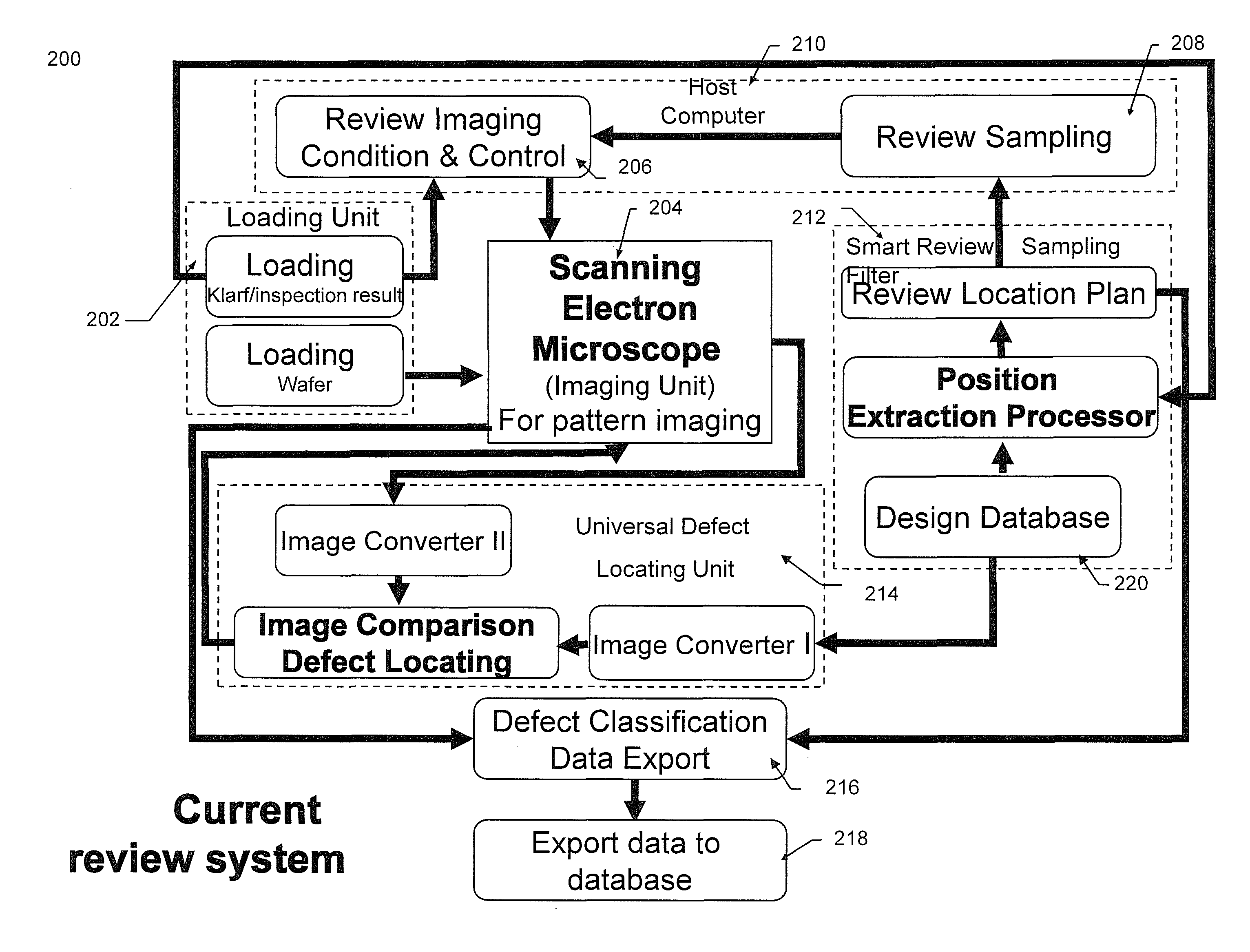
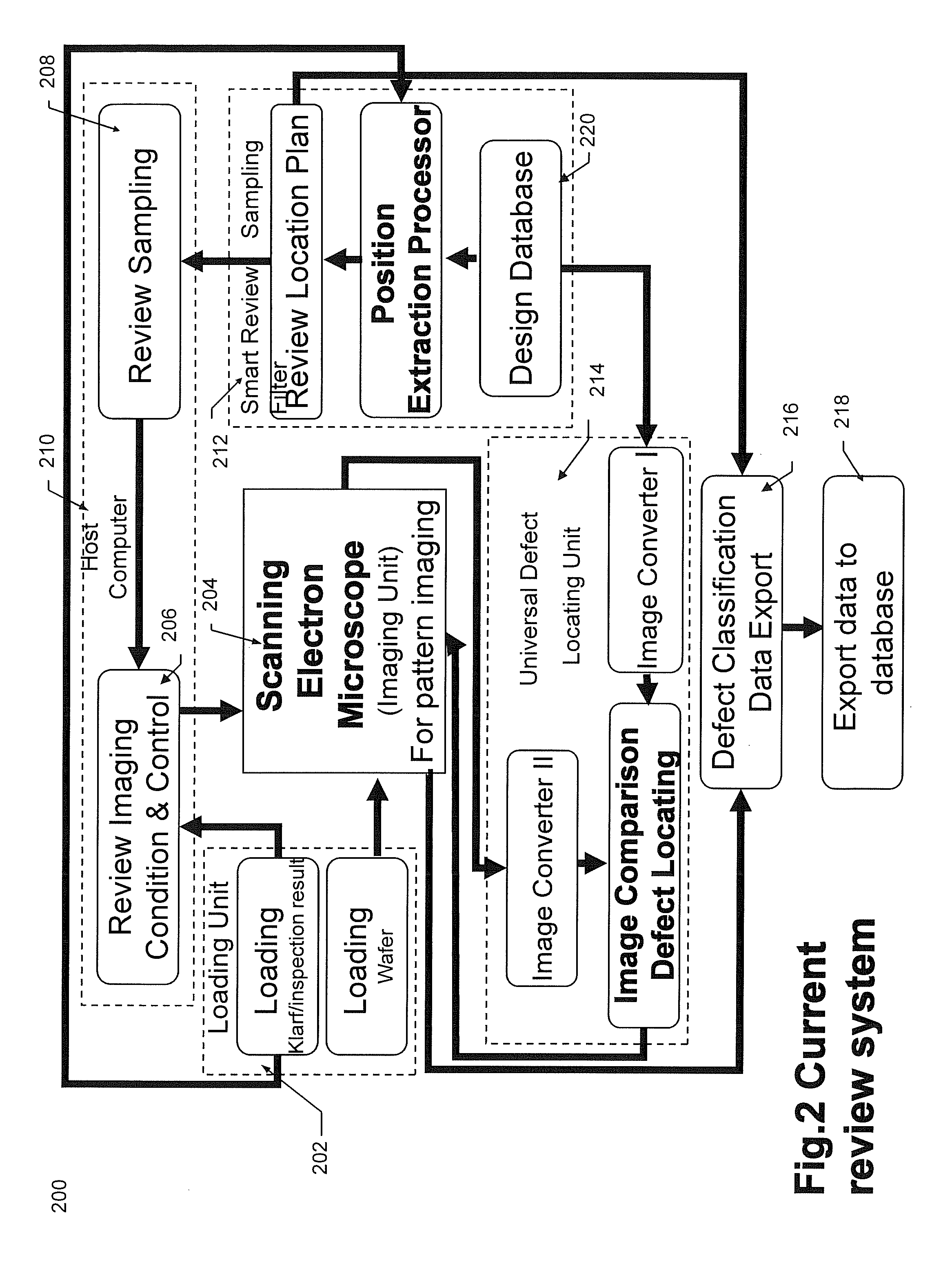
[0008]This and other objects are achieved in comparing a reviewed image with a reference image pick-up through a smart sampling filter. In one embodiment, a clustering computer system is disclosed, the system based on high speed network will provide data cache and save operation time and memory. In another embodiment, a smart review sampling filter is disclosed, the smart review sampling filter automatically relocate abnormal pattern or defects and classify the device location extracted from design database and / or from golden die image on the same substrate. An additional function to enhance the processing speed is that care areas according to the customer predetermined defect of interest (DOI) are loaded into the host computer to screen out defects that are not fall in the care areas.
[0009]The column of the present defect review system adopts the modified SORIL type objective lens to ameliorate aberration at large field of view and under electric drifting. This column provides solution of improving throughput during sample inspection, review or material identification by utilizing fast scanning ability of SORIL and provides a large voltage difference between sample and detectors. This design makes the secondary electrons impinging on the detector with large kinetic energy which is better for getting higher detection gain. Thereafter provide higher signal to noise ratio to benefit image quality. In addition, the column also provides solution of topography analysis by adopting and modifying multi-channels detector and provides material analysis with equipped EDS.
[0011]The present invention provide a defect review system with smart review sampling filter to locate the defect more efficiently, a review station column that can provide stereo image with high resolution, an auxiliary optical grating focusing accessory to enhance micro-defocusing according surface topography, equip with EDS for material analysis ability and a surface charge regulation method to meet these needs.

Problems solved by technology

Defects can occur on the mask or wafer during the semiconductor fabrication process, which impact yield to a great degree.
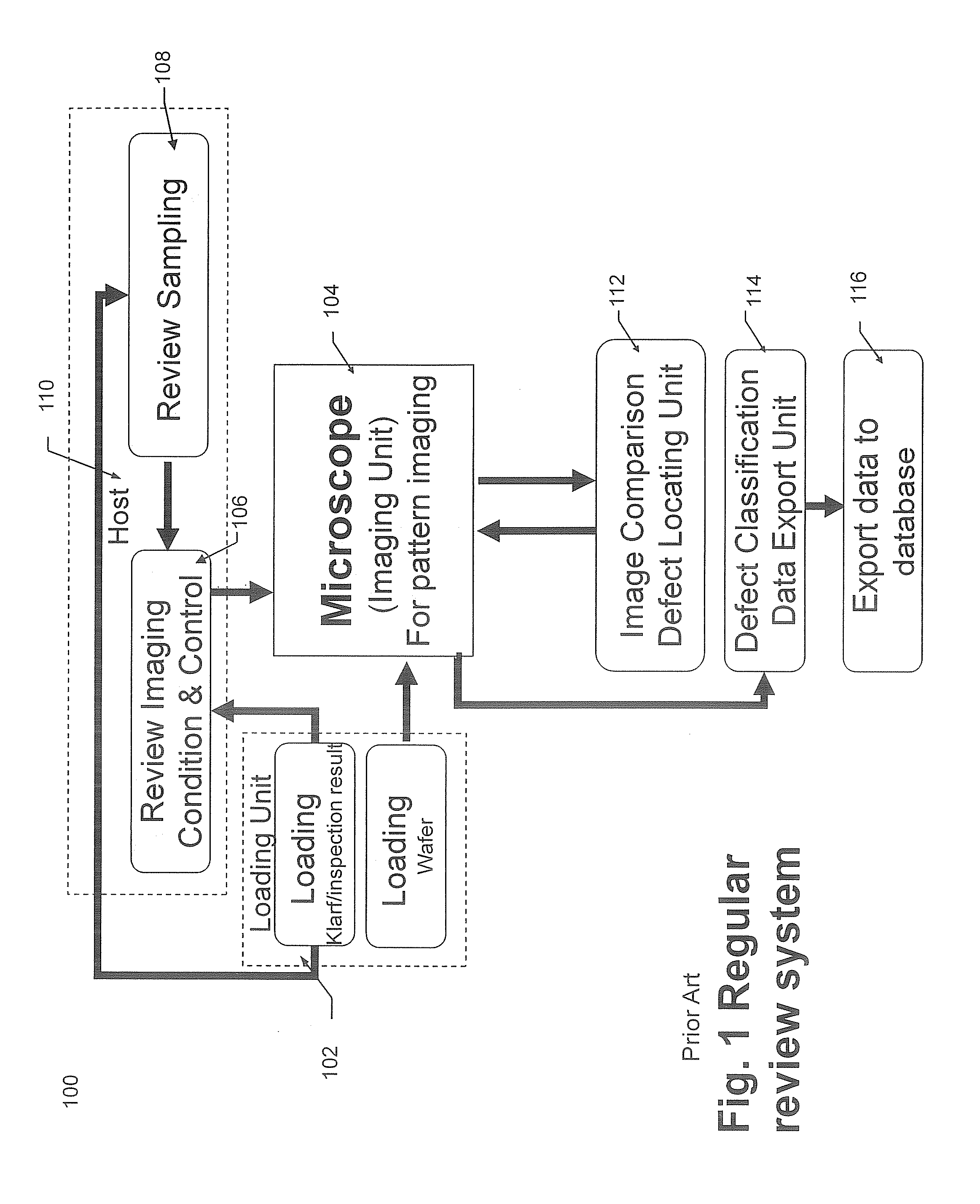
However, an electron beam (e-beam) defect review station is not only receiving defect maps from electron beam inspection system but in the most cases also receiving defect maps from optical defect inspection system.
In addition, wafer surface charging due to electron impinging sample surface is another issue that affecting imaging quality.
After loading the defect map, automatic defect locating (ADL), defect review and defect classification (die to die comparison or die to database comparison) are very complicated and time consuming.

Method used


Image

  • E-beam defect review system
  • E-beam defect review system
  • E-beam defect review system

Examples


Embodiment Construction

[0021]Reference will now be made in detail to specific embodiments of the invention. Examples of these embodiments are illustrated in accompanying drawings. While the invention will be described in conjunction with these specific embodiments, it will be understood that it is not intended to limit the invention to these embodiments. On the contrary, it is intended to cover alternatives, modifications, and equivalents as may be included within the spirit and scope of the invention as defined by the appended claims. In the following description, numerous specific details are set forth in order to provide a thorough understanding of the present invention. The present invention may be practiced without some or all of these specific details. In other instances, well known process operations are not described in detail in order not to unnecessarily obscure the present invention.

[0022]The present invention relates to a defect review system, and / or particularly, to an apparatus and method of...


PUM


Abstract

An apparatus comprises an imaging unit to image a wafer to be reviewed, wherein imaging unit is the modified SORIL column. The modified SORIL column includes a focusing sub-system to do micro-focusing due to a wafer surface topology, wherein the focusing sub-system verifies the position of a grating image reflecting from the wafer surface to adjust the focus; and a surface charge control to regulate the charge accumulation due to electron irradiation during the review process, wherein the gaseous molecules are injected under a flood gun beam rather than under a primary beam. The modified SORIL column further includes a storage unit for storing wafer design database; and a host computer to manage defect locating, defect sampling, and defect classifying, wherein the host computer and storage unit are linked by high speed network.

Description

CROSS-REFERENCES TO RELATED APPLICATIONS[0001]This application relates to U.S. patent application Ser. No. 12 / 024,033, filed Jan. 31, 2008, entitled “Smart Defect Review for Semiconductor Integrated Circuit”; U.S. patent application Ser. No. 12 / 257,304, filed Oct. 23, 2008, entitled “A Charged Particle Beam Apparatus”, now U.S. Pat. No. 7,960,697, entitled Electron Beam Apparatus,; U.S. patent application Ser. No. 11 / 759,138, filed in Jun. 6, 2007, entitled “Optical Auto Focusing System and Method for Electron Beam Inspection Tool”, now U.S. Pat. No. 7,767,982; and U.S. patent application Ser. No. 12 / 232,834, filed Sep. 25, 2008, entitled “Method for Regulating Scanning Sample Surface Charge in Continuous and Leap-and-Scan Scanning Mode Imaging Process” now U.S. Pat. No. 7,973,283.FIELD OF THE INVENTION[0002]The present invention relates to a defect review system, and / or particularly, to an apparatus and method of defect review sampling, review method and classification on a semicon...

Claims


Application Information

Patent Timeline
Patent Type & Authority Patents(United States)
IPC IPC(8): G06K9/00
CPCG01N23/04G06T7/001G01N2223/102G01N2223/426G01N2223/611G06T2207/10061G06T2207/30148H01J37/28H01J2237/2817H01J2237/216H01J2237/0044
Inventor JAU, JACKCHEN, ZHONGWEIWANG, YI XIANGPAN, CHUNG-SHIHWANG, JOELIU, XUEDONGREN, WEIMINGFANG, WEI
Owner ASML NETHERLANDS BV
Why Eureka
Try Eureka