Apparatus and method for measuring structures on a mask and or for calculating structures in a photoresist resulting from the structures

a technology of structures and masks, applied in the field of apparatus for measuring structures on masks and calculating structures in photoresists on wafers, can solve the problems of different results of measuring devices, measurement and measuring devices are not suitable for determining

Active Publication Date: 2012-01-24
VISTEC SEMICON SYST
View PDF15 Cites 0 Cited by
  • Summary
  • Abstract
  • Description
  • Claims
  • Application Information

AI Technical Summary

Benefits of technology

[0016]It is therefore an object of the present invention to provide an apparatus which allows for determining the positions and structural widths of structures on a mask, wherein the apparatus should also be suitable to calculate the result of a structure on the mask printed by a stepper.
[0018]It is another object of the present invention to provide a method allowing positions and structural widths of structures on a mask to be determined, wherein the method should also be suitable to calculate the result of a structure on a mask printed by means of a stepper.
[0028]In further embodiments, the lenses are arranged on a slide or a turret, so that they can be quickly and easily exchanged for each necessary application—measuring the structures on a mask or calculating the structures resulting in the photoresist on the wafer. The apparatus according to the present invention is not limited to these two elements, rather, further elements are conceivable which could be used to exchange the lenses without departing from the scope of protection of the invention.
[0038]The immediate comparison of measuring values with different illuminations under otherwise the same evaluation conditions therefore allows an extended analysis of the mask manufacturing processes. Further advantages of the apparatus according to the present invention and the method according to the present invention can be derived. The cost for checking defective structures on the mask or in the photoresist on the wafer is reduced, since no external checking measuring device, such as the AIMS, is necessary. The checking method with respect to defective structures is simplified, since all steps of the above described method are within one and the same process line. Since the substrate / the wafer / the mask is no longer transferred between two different apparatuses, the risk of destruction of the substrate / the wafer / the mask during handling is reduced.

Problems solved by technology

The measuring device is not suited, however, to determine how the structures on the substrate (mask) are ultimately imaged in the photoresist on the wafer by the stepper.
The evaluation of the measuring results for a structure width measurement can lead, however, to different results in different measuring devices.
These measuring devices are not for determining the position coordinates of the structural elements.
While it is possible with the suggested method, unlike prior art methods, to correct effectively mask structures for manufacturing large-scale integrated circuits, computation overhead is considerable.
A further drawback of this method is the great number of parameters to be taken into account in the form of correction values.

Method used


Image

  • Apparatus and method for measuring structures on a mask and or for calculating structures in a photoresist resulting from the structures
  • Apparatus and method for measuring structures on a mask and or for calculating structures in a photoresist resulting from the structures
  • Apparatus and method for measuring structures on a mask and or for calculating structures in a photoresist resulting from the structures

Examples


first embodiment

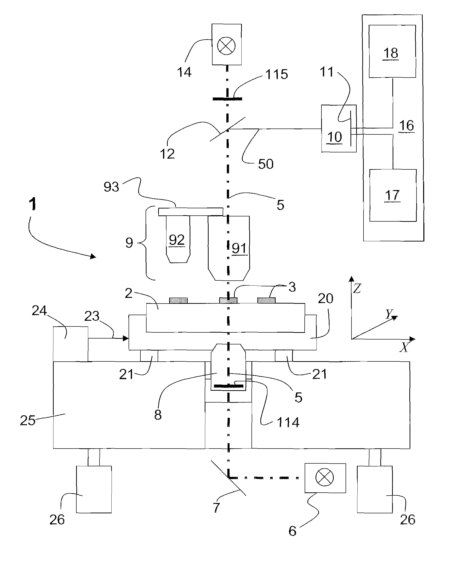
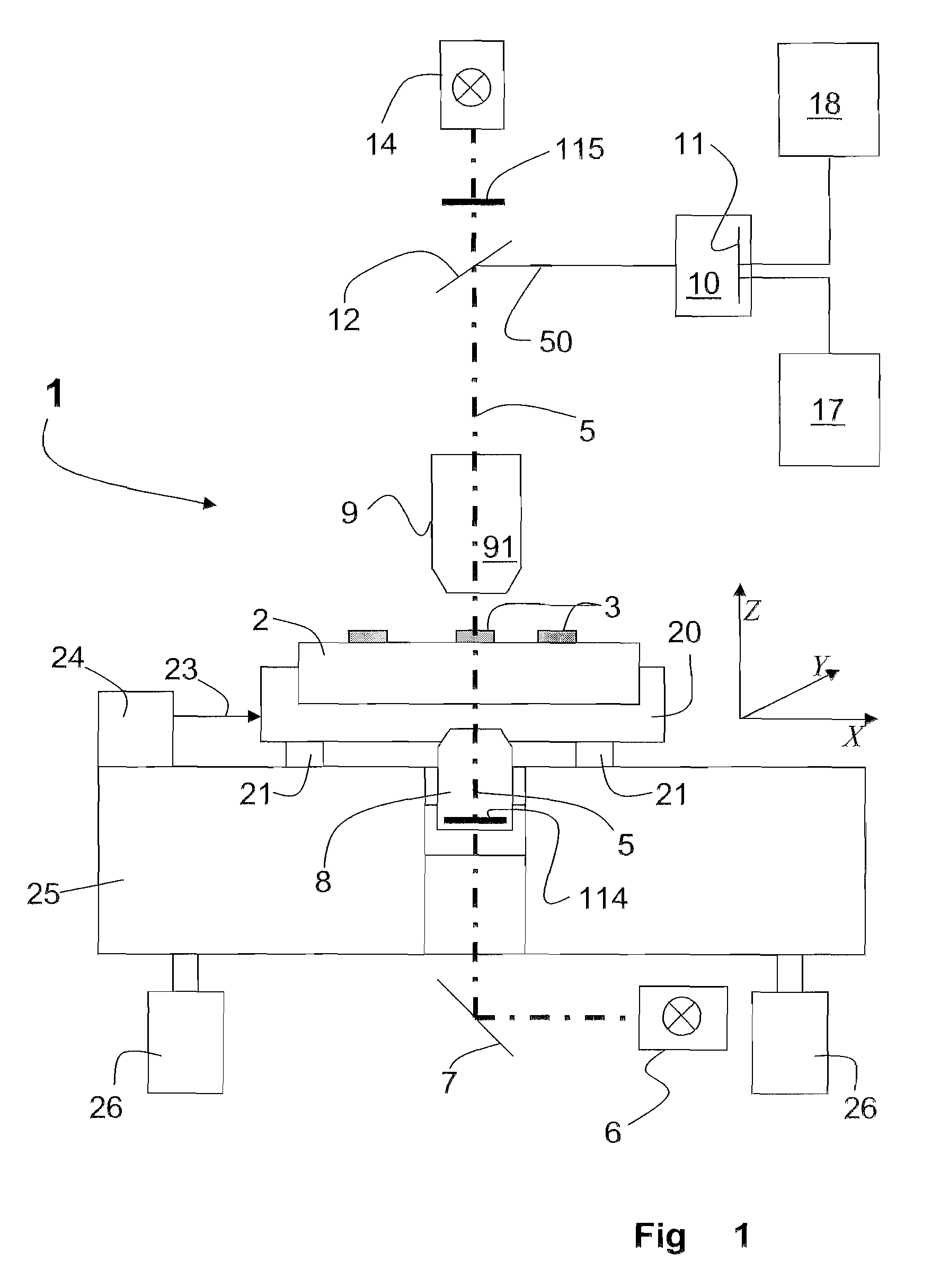
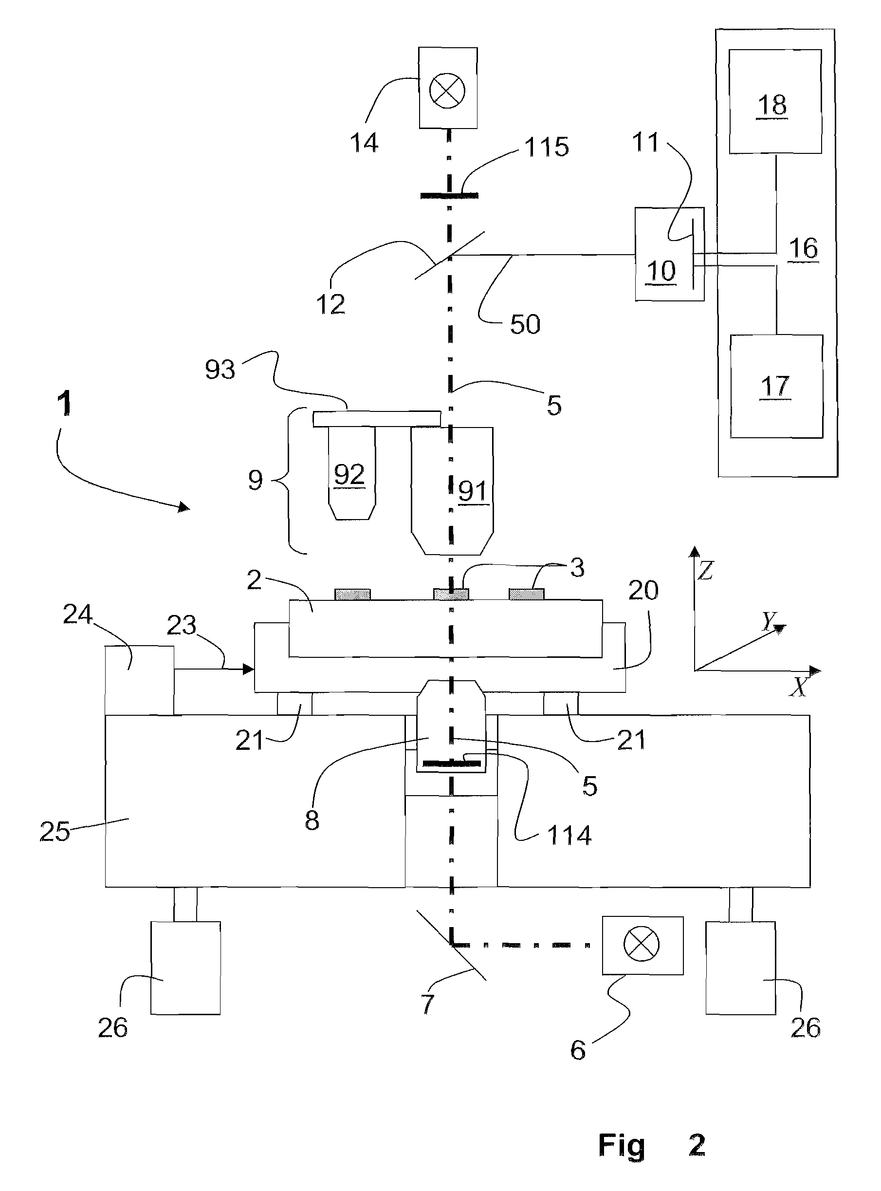
[0044]FIG. 1 is a schematic view of apparatus 1 according to the present invention, which is a coordinate measurement machine, as it has been known for some time from the prior art for measuring structures 3 on masks and / or wafers. The exemplary embodiment shown in FIG. 1 of apparatus 1 allows substrates to be optically inspected and measured. The substrate according to the present invention is a mask 2, for example of quartz glass. Mask 2 is used for the manufacturing of semiconductors, such as wafers. A plurality of structures 3 are applied to mask 2, which can be measured with the aid of apparatus 1. Apparatus 1 comprises an optical axis 5. A transmitted-light illumination means 6 is provided for the transmitted-light mode, which emits light in the near UV or DUV and passes the light via a mirror 7 towards a condenser 8. The light in optical axis 5 passes through substrate 2 and is at least substantially collected by an imaging optics 9 having a lens 91 and imaged onto a detector...

second embodiment

[0051]FIG. 2 shows the invention configured according to FIG. 1. In addition to lens 91, imaging optics 9 of apparatus 1 comprises at least one further lens 92. The at least two lenses 91, 92 are arranged on a slide 93 in the embodiment shown in FIG. 2. Depending on each wavelength used, this is how a suitable lens 91 or 92 can be brought into the beam path of optical axis 5 of apparatus 1. If the position and / or the CD of the structures on a mask 2 are to be determined, a wavelength in the near UV range or light of the wavelength of equal to or smaller than 400 nm is used, which is larger than the wavelength used in the stepper. If the printed pattern is to be evaluated, i.e. the structure to be expected in the photoresist on the wafer is to be calculated, lens 91 or 92 formed for the wavelength to be used in a stepper, is brought into the beam path of the apparatus.


PUM

PropertyMeasurementUnit
wavelengthaaaaaaaaaa

Abstract

An apparatus (1) for measuring structures (3) on a mask (2) and for calculating structures in a photoresist on a wafer resulting from the structures (3) on the mask (2) is disclosed, wherein the apparatus (1) comprises at least one incident-light illumination means (14) and / or one transmitted-light illumination means (6), wherein the apparatus (1) comprises at least one imaging optics (9) and a detector (11) of a camera (10) for imaging the structures (3) on the mask (2), wherein a first computer program (17) is associated with the detector (11) of the camera (10) and provided for determining the position and / or the dimension of the structure (3) on the mask (2). A method for measuring structures (3) on a mask (2) and for calculating structures in a photoresist on a wafer to be expected from the structures (3) on the mask (2) is also disclosed.

Description

RELATED APPLICATIONS[0001]This application claims priority to German Patent Application No. DE 10 2007 009 254.9, filed on Feb. 22, 2007, and German Patent Application No. DE 10 2007 000 981.1, filed on Nov. 7, 2007, and claims the benefit under 35 USC 119(e) of U.S. Provisional Application No. 60 / 891,164 filed on Feb. 22, 2007, all of which are incorporated herein by reference in their entirety.BACKGROUND OF THE INVENTION[0002]The present invention relates to an apparatus for measuring structures on a mask and for calculating the structures in a photoresist on a wafer resulting from the structures on the mask.[0003]The present invention further relates to a method for measuring structures on a mask and for determining the structures in a photoresist on a wafer resulting from the structures on the mask.[0004]A measuring device according to the prior art measures structures on a substrate, wherein the measuring device comprises incident-light and / or transmitted-light illumination mea...

Claims


Application Information

Patent Timeline
Patent Type & Authority Patents(United States)
IPC IPC(8): G01B11/14G03F1/00
CPCG01B11/03G03F1/84
Inventor HEIDEN, MICHAEL
Owner VISTEC SEMICON SYST
Why Eureka
Try Eureka