
Method and device for connecting a wiring board

a technology of anisotropic conductive film and connection method, which is applied in the direction of metal working apparatus, printed circuit manufacturing, manufacturing tools, etc., can solve the problems of increasing the distance between the anisotropic conductive film and excessive load on the mounting electronic component, and damage to the electronic component, so as to achieve high reliability and connection state, enhance the mounting density of the component, and avoid the possibility of disadvantages of mounting electronic components

Inactive Publication Date: 2012-02-07
DEXERIALS CORP
View PDF6 Cites 0 Cited by
  • Summary
  • Abstract
  • Description
  • Claims
  • Application Information

AI Technical Summary

Benefits of technology

The present invention provides a wiring board receiving panel and a device for connection of wiring boards that use an elastic material for stable support of electronic components during thermal compression bonding. This ensures uniform thermal conductive bonding and prevents damage to the mounted electronic component. The invention also allows for flexible mounting of electronic components on the rear surface of a motherboard substrate, increasing component mounting density and reducing the size, weight, and thickness of the wiring board.

Problems solved by technology

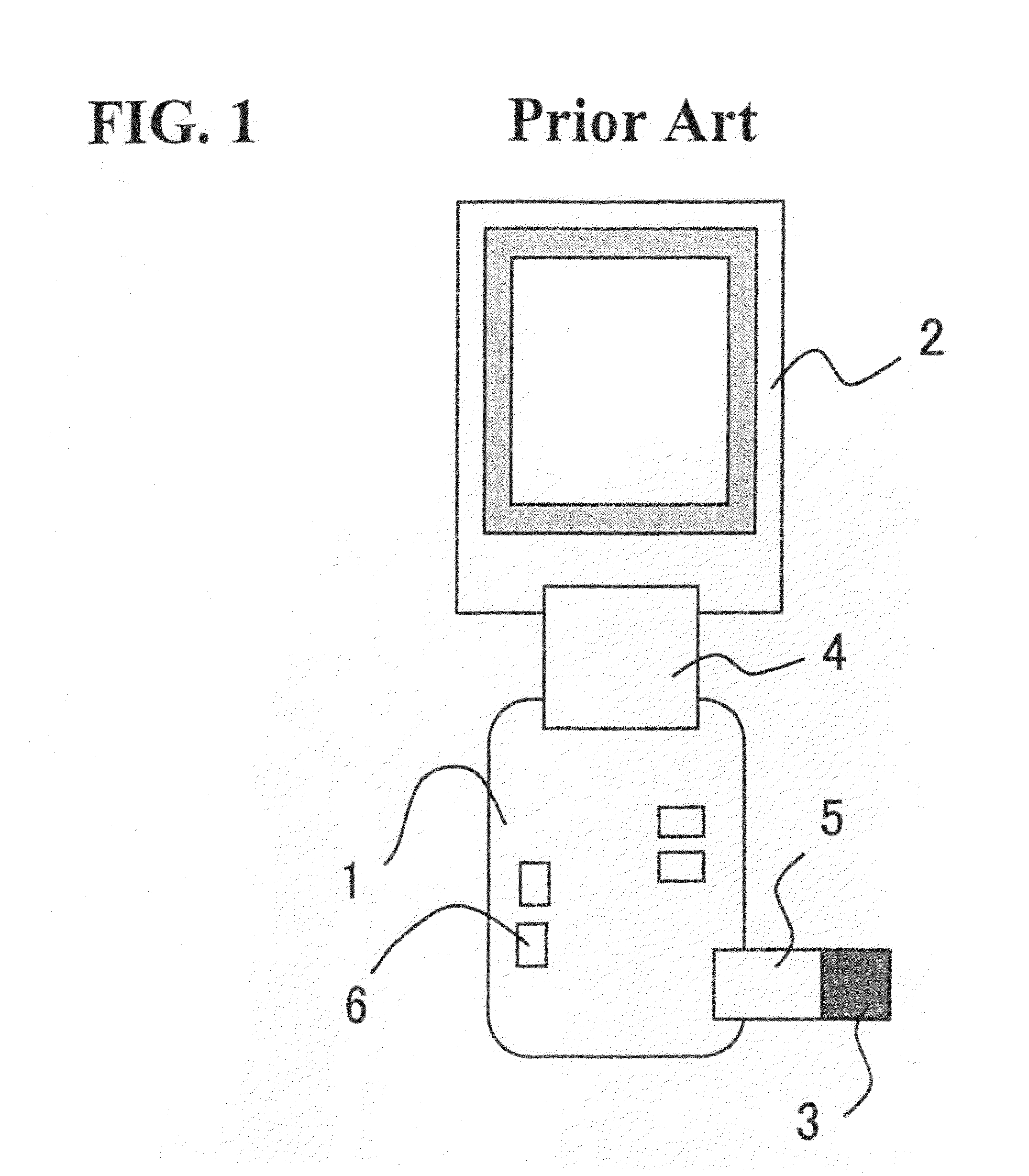
However, in association with equipment lightweight, thin and small in size, connection by the anisotropic conductive film tends to be increasing.
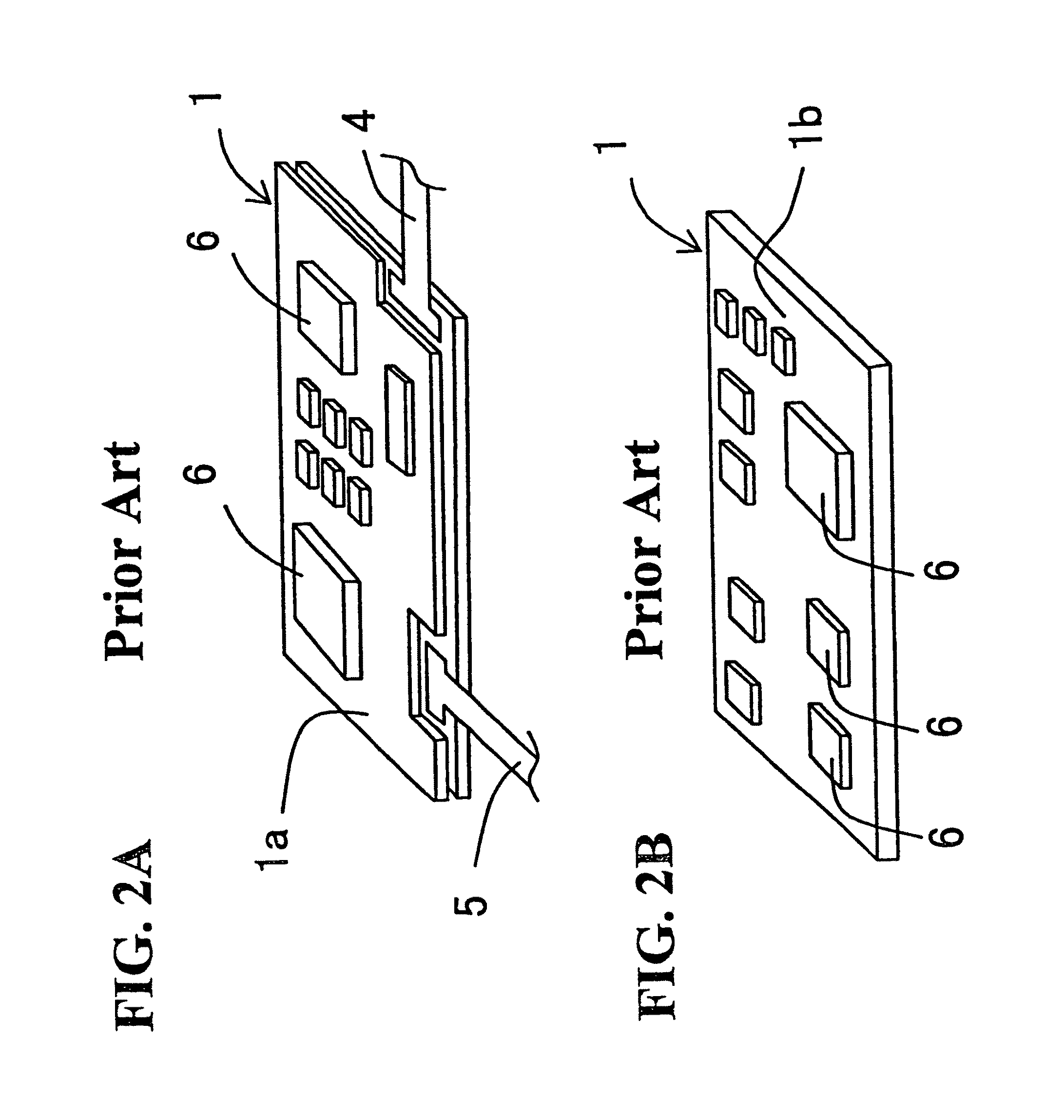
This is because, when performing the thermal compression bonding, with the portion having mounted the electronic component supported on the rear surface side of the motherboard substrate, there is a possibility of entailing problems of applying uneven pressure, exerting an excessive load on the mounted electronic component and consequently damaging the electronic component.
In this case, mounting of the electronic component on the motherboard substrate is subjected to restraints including a requirement that the component be disposed in consideration of the connection by the anisotropic conductive film and, therefore, a problem of lowering the component-mounting area ratio is imposed.
In the supporting structure of the invention described in Patent Document 2, however, since only the surroundings of the wiring board and mounting component are supported, it is difficult to stably support the wiring board and problems of flexing the wiring board at the time of thermal compression bonding, damaging the wiring board and applying uneven pressure to the wiring board to induce bad connection will remain.
In addition, an increase in number of electronic components to be mounted on the wiring board makes the structure of the substrate-retaining member complicated and necessitates great equipment investment.
These are also problematic.
Though this is somewhat expected to exhibit effectiveness to some extent, since the substrate-supporting body that supports the outer peripheral portion can only supports the lower surface of the substrate, it is difficult to realize a stable support state similarly to the invention described in Patent Document 2.
In addition, since only the electronic component that has already been mounted is supported on the elastic body at the position on which pressure loads are actually exerted, excessive load is added consequently to the already-mounted electronic component.
Particularly, when the difference in mounting height of the electronic components to be mounted is large, it is difficult to uniformly applying pressure even in the presence of the elastic body and to completely eliminate damages of the already-mounted electronic components.

Method used


Image

  • Method and device for connecting a wiring board
  • Method and device for connecting a wiring board
  • Method and device for connecting a wiring board

Examples


example 1

[0047]A printed-wiring board (corresponding to the first wiring board) formed with electrode terminals having a pitch of 200 μm, in which L / S=100 μm / 100 μm, and a flexible printed circuit board (corresponding to the second wiring board) were prepared and connected to each other with an ACF using a receiving plate made of silicon rubber (silicone rubber). Incidentally, concave portions corresponding in number to electronic components mounted on the printed-wiring board were formed in the receiving plate made of the silicon rubber. The rubber hardness degree of the receiving plate made of the silicon rubber was 40. In addition, as the anisotropic conductive film, that produced by Sony Chemical & Information Device Corporation and sold under the trade name of CP5842KS was used. As the thermal compression bonding head, a heater built-in head was used to perform heating and pressure application.

example 2

[0048]A printed-wiring board and a flexible printed circuit board were connected to each other with an ACF in the same manner as in Example 1, except that the rubber hardness degree of the receiving plate made of silicon rubber was set to be 90.

example 3

[0049]A printed-wiring board and a flexible printed circuit board were connected to each other with an ACF in the same manner as in Example 1, except that the rubber hardness degree of the receiving plate made of silicon rubber was set to be 20.


PUM

PropertyMeasurementUnit
height H1aaaaaaaaaa
elasticaaaaaaaaaa
heightaaaaaaaaaa

Abstract

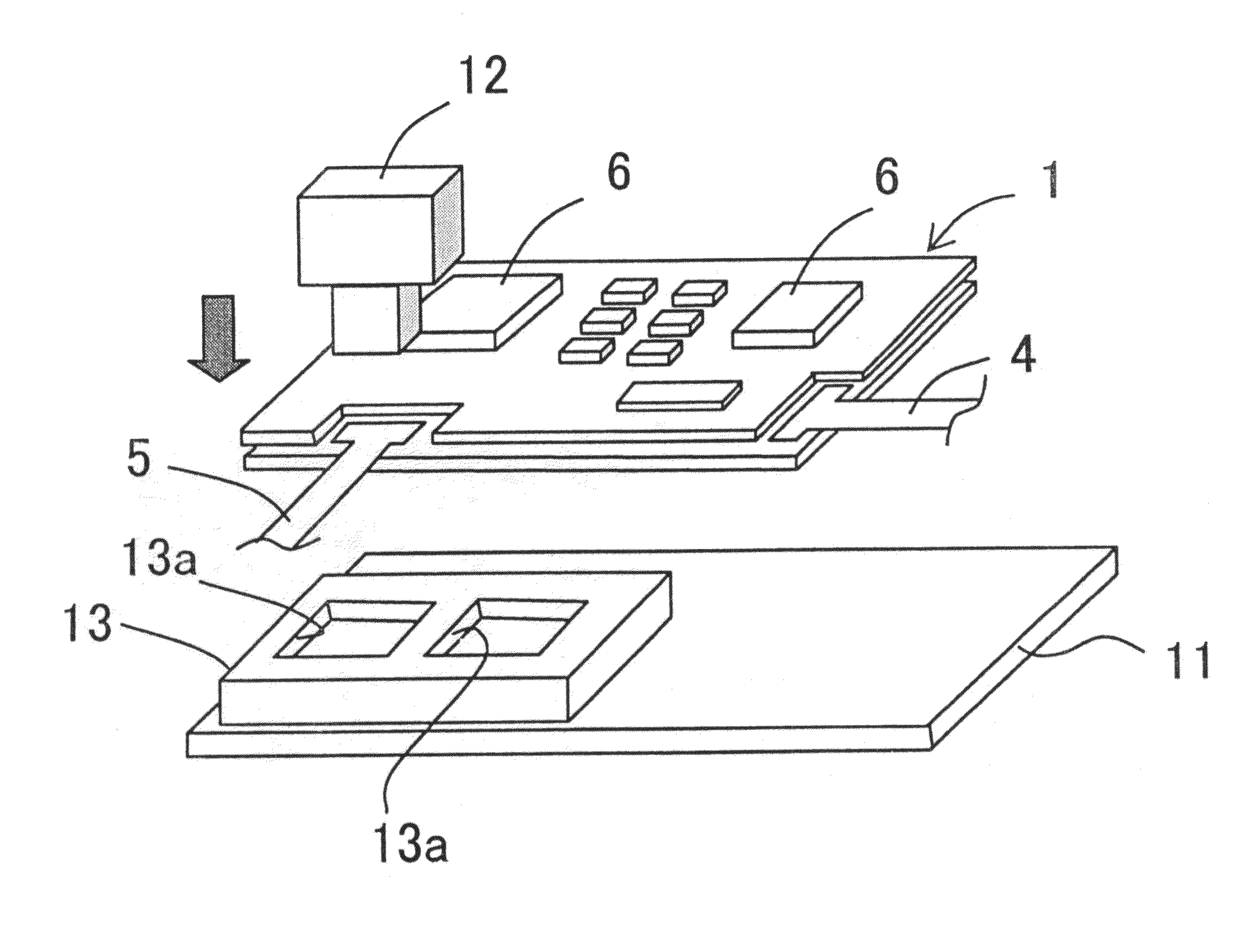
Connection with an ACF is realized relative to a wiring board having an electronic component mounted on the rear surface thereof with high connection reliability and uniform thermal compression bonding. A thermal compression bonding head 12 is used to apply pressure to flexible printed circuit boards 4 and 5 relative to a motherboard substrate 1 having an electronic component 6 mounted thereon and heat an anisotropic conductive film, thereby connecting the motherboard substrate 1 with the ACF to the flexible printed circuit boards 4 and 5 that are connecting members. At this time, in a state in which a receiving plate 13 made of an elastic material, such as silicone rubber, and provided at a mounting position of the electronic component 6 of the motherboard substrate 1 with a concave portion 13a corresponding in shape to the electronic component 6 supports thereon the rear surface of the motherboard substrate 1, the thermal compression bonding is performed.

Description

RELATED APPLICATIONS[0001]The present application is National Phase of International Application No. PCT / JP2008 / 065944 filed Sep. 4, 2008 and claims priority from, Japanese Application No. 2007-275184 filed Oct. 23, 2007, the disclosure of which is hereby incorporated by reference herein in its entirety.BACKGROUND OF THE INVENTION[0002]1. Field of the Invention[0003]The present invention relates to a wiring board receiving plate used in connecting a wiring board or electronic component to a different wiring board having an electronic component mounted thereon and further to a connection device and method of a wiring board using the receiving plate.[0004]2. Description of the Prior Art[0005]In mounting a semiconductor device on a wiring board, for example, the flip-chip mounting method for mounting it on the wiring board in a so-called face-down state has been proposed and, for electrical connection between electrodes and for physical fixation of the semiconductor device, an anisotro...

Claims


Application Information

Patent Timeline
Patent Type & Authority Patents(United States)
IPC IPC(8): H05K3/36
CPCH05K3/361H05K3/323H05K2203/0173H05K2203/0195H05K2203/0278Y10T29/49144Y10T29/4913Y10T29/49126Y10T29/5317
Inventor SAITO, MASAO
Owner DEXERIALS CORP
Learn More