Imprint device and microstructure transfer method

a technology of imprint device and microstructure, which is applied in the direction of photomechanical equipment, applications, instruments, etc., can solve the problems of increasing the cost of the device, increasing the complexity of the configuration of the imprint device, and approaching the limit of the high accuracy of the pattern formation process

Inactive Publication Date: 2012-02-07
HITACHI HIGH-TECH CORP
View PDF16 Cites 7 Cited by
  • Summary
  • Abstract
  • Description
  • Claims
  • Application Information

AI Technical Summary

Benefits of technology

[0013]The present invention was made to solve the problems as described above, and it is an object of the present invention to provide an imprint device and a microstructure transfer method, by which it is possible to sufficiently spread a resin or other material for forming a pattern layer between a stamper and a patterned material with a lower pressure so as not to damage the stamper or the patterned material, and to form a pattern formation layer having the uniform thickness on the patterned material.
[0016]With the imprint device and the microstructure transfer method of the present invention, it is possible to sufficiently spread a resin or other material for forming a pattern layer between a stamper and a patterned material with a lower pressure so as not to damage the stamper or the patterned material, and to form a pattern formation layer having the uniform thickness on the patterned material.

Problems solved by technology

On the other hand, a pattern for the microfabrication process is almost as small as a wavelength of an exposure light source, and therefore the microfabrication process is approaching to a limit for the high accuracy of the pattern formation.
However, the electron beam lithography device, which uses the batch drawing radiation method, increases in size and requires a mechanism for controlling a position of a mask with higher accuracy, thereby increasing the cost of the device.
However, the above-described imprint device requires an adjustment mechanism capable of aligning the stamper and the patterned material parallel to each other with high accuracy, thereby making a configuration of the imprint device complicated.
Furthermore, in the imprint device, there is a limit on the size of the stamper to be able to be made flat, and it is difficult to form the pattern formation layer (thin film layer) having the uniform thickness by pressing a larger size of the patterned region against the stamper at one time.
Therefore, it is difficult to sufficiently spread the resin between the stamper and the patterned material when the patterned region is larger and the thin film layer is thinner.
In this case, the stamper and the patterned material can be damaged when the stamper is pressed against the patterned material with a higher pressure to spread the resin between the stamper and the patterned material.

Method used


Image

  • Imprint device and microstructure transfer method
  • Imprint device and microstructure transfer method
  • Imprint device and microstructure transfer method

Examples


first embodiment

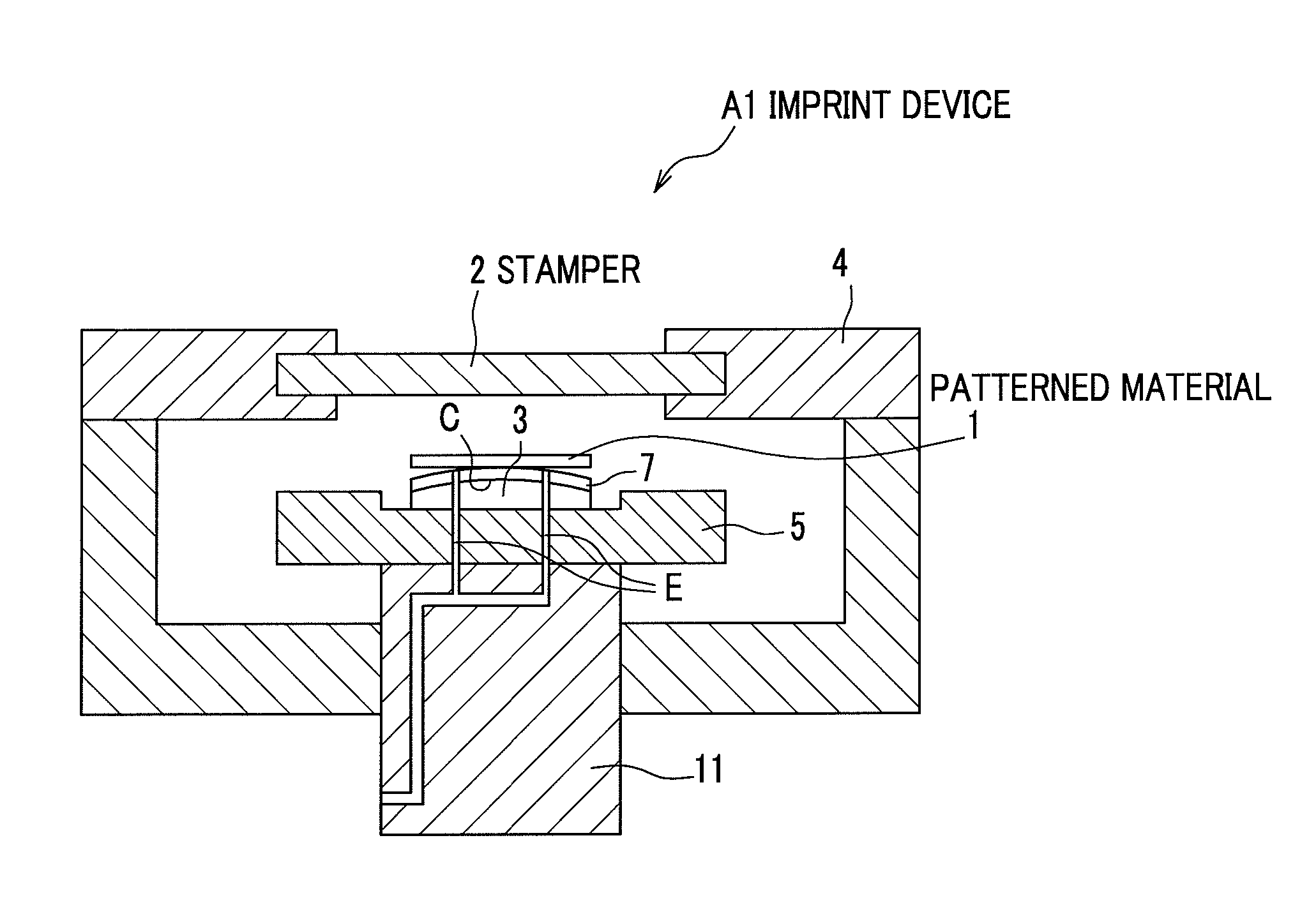
[0033]Detailed description will be provided for a first embodiment of the present invention with reference to the attached drawings. FIG. 1 illustrates a configuration of an imprint device according to the first embodiment.

[0034]As shown in FIG. 1, an imprint device A1 of the first embodiment includes an up-down mechanism 11, a stage 5 that is moved up and down by the up-down mechanism 11, a plate 3, and a buffer layer 7. The plate 3 and the buffer layer 7 are disposed on the stage 5 in order. The imprint device A1 includes air intake paths E connected to a suction unit (not shown) such as a pump. Each of the air intake paths E passes through the inside of the up-down mechanism 11, the stage 5, the plate 3, and the buffer layer 7, and has an opening at the upper surface of the buffer layer 7. An opening of the air intake path E on the opposite side of the buffer layer 7 is connected to the above-described suction unit. A patterned material 1 is disposed on the plate 3 through the bu...

second embodiment

[0056]Next, detailed description will be provided for a second embodiment of the present invention with reference to the attached drawings. Of the drawings to be referred to, FIGS. 3A and 3B illustrate an imprint device according to the second embodiment. FIG. 3A illustrates a configuration of an imprint device, and FIG. 3B schematically illustrates an arrangement of openings of flow paths provided in an imprint device. In the imprint device according to the second embodiment, a configuration of a plate arranged on a stage is different from that of the plate according to the first embodiment, and therefore description will be mainly provided for the configuration of the plate of the second embodiment.

[0057]In an imprint device A2 of the second embodiment, as shown in FIG. 3A, a plate 3 has the flat upper surface on the side to face the stamper 2. A buffer layer 7 is disposed on the flat upper surface of the plate 3, and the buffer layer 7 also has a flat upper surface. The imprint d...

example

[0070]Next, the present invention will be described in more detail by illustrating examples of the present invention.


PUM

PropertyMeasurementUnit
widthaaaaaaaaaa
thicknessaaaaaaaaaa
depthaaaaaaaaaa

Abstract

There is provided an imprint device for transferring a fine pattern to a material to form a patterned material. The device comprises a stamper having the fine pattern thereon, and a pressure distribution mechanism. The stamper is pressed against the material, and the pressure distribution mechanism provides a nonuniform pressure distribution in a patterned region of the patterned material, while the stamper is in contact with the material. There are provided an imprint device and a microstructure transfer method, by which it is possible to sufficiently spread a resin or other material for forming a pattern layer between a stamper and a patterned material with a lower pressure so as not to damage the stamper or the patterned material, and to form a pattern formation layer having the uniform thickness on the patterned material.

Description

CROSS-REFERENCE TO RELATED APPLICATION(S)[0001]This application claims the foreign priority benefit under Title 35, United States Code, §119(a)-(d), of Japanese Patent Application No. 2006-187958 filed on Jul. 7, 2006 in the Japan Patent Office, the disclosure of which is herein incorporated by reference in its entirety.BACKGROUND OF THE INVENTION[0002]1. Field of the Invention[0003]The present invention relates to an imprint device and a microstructure transfer method for transferring a fine-patterned structure of a stamper to a surface of a patterned material.[0004]2. Description of the Related Art[0005]Microfabrication of semiconductor integrated circuits has progressed and there has been improvement in the accuracy for forming a pattern of a semiconductor integrated circuit by, for example, the photolithography device in order to perform the microfabrication process. On the other hand, a pattern for the microfabrication process is almost as small as a wavelength of an exposure l...

Claims


Application Information

Patent Timeline
Patent Type & Authority Patents(United States)
IPC IPC(8): B28B11/08
CPCB29C43/003B29C43/021B29C43/58B82Y10/00B82Y40/00G03F7/0002B29C2043/025B29C2043/3634B29C2043/5808B29L2011/0016
Inventor ANDO, TAKASHIKOMORIYA, SUSUMUOGINO, MASAHIKOMIYAUCHI, AKIHIRO
Owner HITACHI HIGH-TECH CORP
Why Eureka
Try Eureka