
Reprogrammable circuit board with alignment-insensitive support for multiple component contact types

a technology of alignment-insensitive support and circuit board, which is applied in logic circuits, printed circuit aspects, instruments, etc., can solve the problems of logic chips that are difficult to apply defect tolerance, the yield of logic chips of this size is very low, and the edge lithography process will average several defects

Inactive Publication Date: 2012-02-28
NORMAN RICHARD
View PDF65 Cites 31 Cited by
  • Summary
  • Abstract
  • Description
  • Claims
  • Application Information

AI Technical Summary

Benefits of technology

[0031]It is therefore one object of the present invention to provide a programmable circuit board larger than a chip package that lets signals from components affixed to it be reprogrammably routed to other components affixed to it without having to route those signals through external programmable interconnect chips affixed to the circuit board.
[0032]It is a further object of the present invention to have a reprogrammable circuit board where substantially all the surface area of and substantially all of the contacts for affixed components are usable for the components of the target system rather than for components to support the reprogrammability, allowing the reprogrammable circuit board to support a system component density comparable to that of a non-programmable printed circuit board.

Problems solved by technology

Even within the area of a reticle image, a leading edge lithography process will average several defects by the time all of the layers are completed.
Since chips the size of a reticle image would thus be very likely to contain at least one defect, the yield of chips this size would be very low.
Memory chips are the most repetitive common chips, and they also have vast arrays of very fine features which make them quite vulnerable to defects; therefore most commercial memory chips contain enough defect tolerance to get acceptable yields at areas of one to two square centimeters, which is still significantly less than the size of a reticle.
Logic chips are harder to apply defect tolerance to because they are typically much less repetitive than memory chips.
First, as discussed above, some systems contain too much non-repetitive logic to make defect tolerance practical.
Second, most systems contain numerous commercially available chips as well as custom circuitry.
Even if one were to accept the technical challenge of replicating those commercial chips in a wafer-scale system, one would still face intellectual property issues in manufacturing them.
While connections between circuits within a chip are on a micron scale, interconnecting circuits on separate chips typically uses a circuit board with millimeter-scale connections, requiring a bulky chip package to connect the chip to the circuit board.
Driving these millimeter or larger scale connections also requires more power, and thus larger drive circuitry, especially since the long interconnections are driven in one shot and can suffer from interference caused by other signals.
Thus while a chip one centimeter square can easily have many tens of thousands of connections from one half to its other half, it will typically be limited to a few hundred or at most a thousand connections to other chips.
However high-end MCMs cost even more to design and prototype than high-end circuit boards do.
However each PCB was now designed and fabricated for a specific task, and while this was simple for simple PCBs, high-performance systems pushed the speed and density of interconnections to the limit, raising the cost of designing each layer and the number of conductive layers needed.
This required a “stack-up’ of many carefully aligned layers of insulator and copper, greatly increasing the time and cost required to produce the PCB.
However the limited capacity of FPICs required multiple stages of these chips for high-end circuit boards, and for full interconnectivity, each stage of FPIC requires as many FPIC contacts as the original system chip contacts that they are interconnecting.
To achieve a high degree of connectivity thus requires several times more area in FPICs than in the chips of the target system, greatly limiting the density of the system chips.
While wire-bonded antifuse-programmable MCMs allow dense connectivity, one-time programmability, and mechanical adaptation to different contact spacings, they do not support releasable attachment of the chips, reusability of the substrate, internal re-driving for signal integrity or retiming for jitter elimination.
While this in not particularly difficult for automated pick-and-place machines during a batch of thousands of identical boards, it is inefficient for one or a few prototypes because it requires the development of a ‘pick-and-place’ program for typically a dozen or more chips and up to several hundred tiny discrete components (with most of these discrete components required for signal integrity).
Since FPIC-based boards are already the most limited in connectivity of the modern prototyping boards, this is a high cost.
For a signal near its maximum noise threshold or near its minimum voltage swing as it leaves a chip, the distance to the test connector or to the FPIC on the way to the test connector may contribute enough extra noise or enough extra attenuation that the signal at the logic analyzer is unreliable.
Because of the possibility of defects within a component and the cost of detecting and locating a defect once a component is installed in a system, and the further cost of replacing defective components if they are non-releasably attached in a system, components are generally tested before they are used.
While testing packaged components is relatively simple, early testing and discarding of defective components saves packaging costs and opens up the possibility of bulk testing.
However additional less-obvious defects may still exist in any component and these typically manifest themselves only after a prolonged ‘burn-in’ period where the features of the component are thoroughly exercised.
These defects include thin spots in wiring that get hotter and thinner over time until they blow like a fuse, and the opposite, where current leaking through an insulator breaks down that insulator, allowing more and more current to flow.
In addition, at the leading edge where the packing of internal features pushes the limits, subtle interactions between signals can produce signal integrity problems that only manifest themselves under extremely specific sets of circumstances, typically including running the circuit at its maximum speed.
Full-wafer at-speed burn-in testing is also known in the art, but it requires a far more complex adapter for each type of component to be tested.
Thus an extremely complex test fixture is necessary merely to make to connections to a wafer full of contacts, and a customized fixture is required for each component's contact pattern.
Carrying all of the outputs from the components through the test jig and back to the tester is far more difficult, as the outputs cannot be assumed to be identical (or there would be no point in testing each component).
However for more complex at-speed testing, to connect the wide address, data and other signal busses of all the chips on a wafer would exceed the capacity of the circuitry attached to a probe card, even with arranging such circuitry out of the plane of the card as taught in U.S. Pat. No. 6,853,206.
Furthermore, adding numerous extra chips to a probe card drives up the cost of the card.

Method used


Image

  • Reprogrammable circuit board with alignment-insensitive support for multiple component contact types
  • Reprogrammable circuit board with alignment-insensitive support for multiple component contact types
  • Reprogrammable circuit board with alignment-insensitive support for multiple component contact types

Examples


Embodiment Construction

First Family of Preferred Embodiments

Reprogrammable Circuit Board with Embedded FPICs

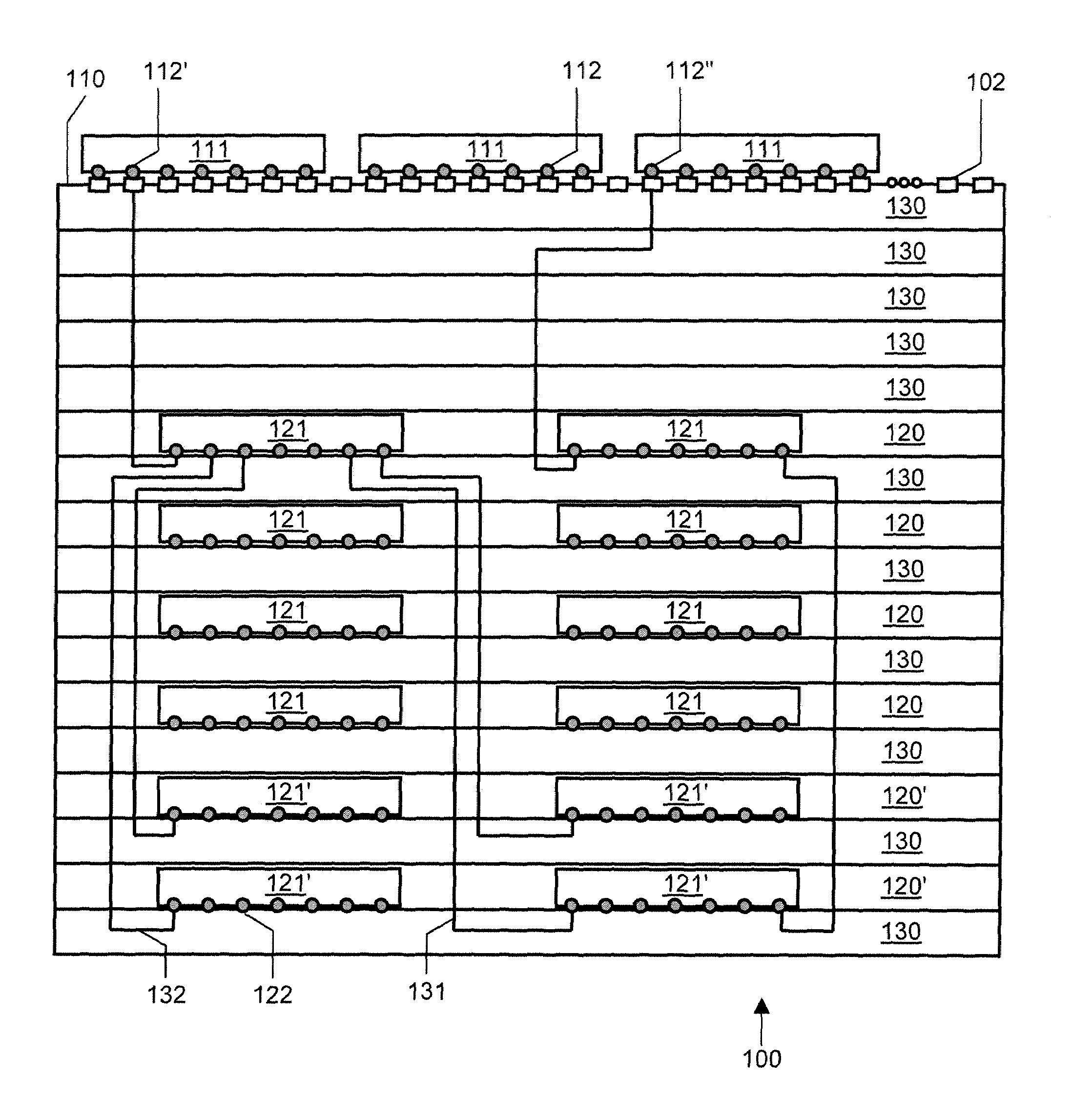
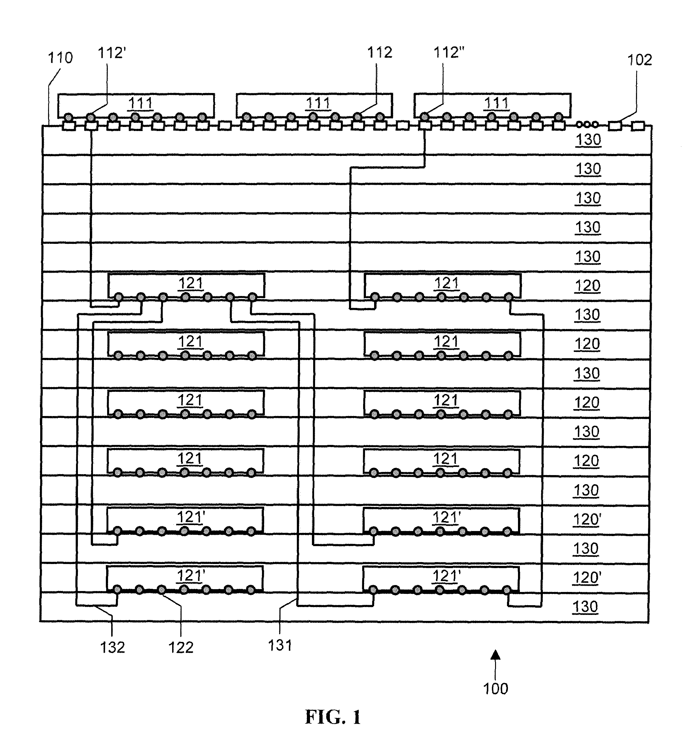
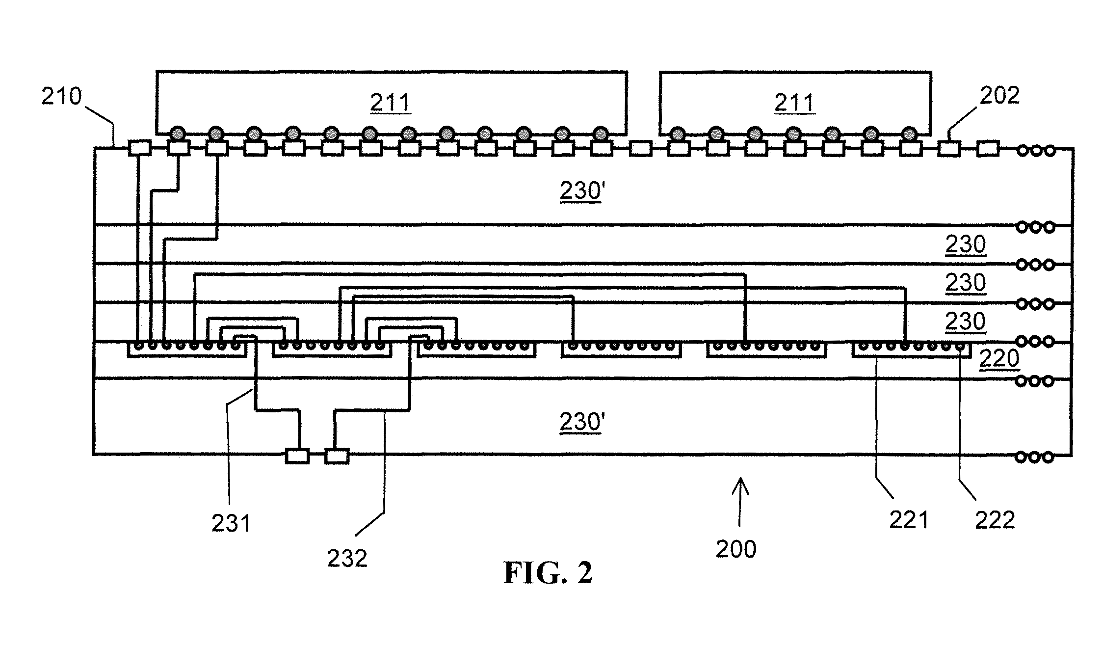
[0188]Printed Circuit Boards, or PCBs, interconnect circuits built on separate chips. However each traditional PCB is designed and fabricated for a specific task, and with high-performance systems pushing the speed and the density of interconnections to the limit, this requires a ‘stack-up’ of many carefully aligned layers, each of which is costly to design.

[0189]The prior art contains numerous examples of attempts to overcome this with multi-purpose circuit boards that can be permanently tailored or programmed for a specific interconnectivity pattern. Programming techniques used range from single masked metal layers (U.S. Pat. No. 5,264,664), to anti-fuses (U.S. Pat. No. 5,490,042). However these techniques are not reversible, so a given PCB cannot be repeatedly tested and modified during the system development cycle.

[0190]To overcome this one-time programmability, reprogrammable circuit boards hav...


PUM

PropertyMeasurementUnit
diameteraaaaaaaaaa
thicknessaaaaaaaaaa
lengthaaaaaaaaaa

Abstract

The present invention is directed to a system that programmably interconnects integrated circuit chips and other components at near-intra-chip density. The system's contact structure allows it to adapt to components with a wide variety of contact spacings and interconnection requirements, the use of releasable attachment means allows component placement to be modified as needed, the system identifies the contacts and the components to facilitate specifying the inter-component connections, and the system provides signal conditioning and retiming to minimize issues with signal integrity and signal skew.

Description

FIELD OF THE INVENTION[0001]The present invention relates to connecting components, such as bare die and / or packaged integrated circuit chips. The invention also relates to tools and methods for prototyping multi-chip systems.SUMMARY OF THE PRIOR ART[0002]Integrated circuit chips are made through a complex lithographic process that builds up patterned layer upon patterned layer. Because circuits with finer lithographic features are denser and run faster than those with coarser features, feature size is pushed into the realm where defects are inevitable. To reduce the number of defects per square centimeter, only a small area of a wafer is exposed to the patterning at any given time so that the whole exposed area fits in the most accurately focused region near the center of focus. After exposure, this area contains the image of a mask that is held in what is called a reticle; therefore this area of the wafer is referred to as a reticle image (sometimes shortened to just a “reticle”)....

Claims


Application Information

Patent Timeline
Patent Type & Authority Patents(United States)
IPC IPC(8): H01L21/02G01R31/02
CPCH01L23/50H01L23/5389H05K1/029H01L23/5382Y10T29/49002H01L25/0652H01L2924/01079H01L2924/12044H01L2924/3011H01L2924/3025H05K1/0298H05K1/185H05K2201/10212H05K2201/10674H01L2224/16225H01L2924/1461Y10T29/53183Y10T29/53174H01L2924/00H01L23/538
Inventor NORMAN, RICHARD
Owner NORMAN RICHARD
Learn More