Laminated ceramic electronic component

a technology of laminated ceramics and electronic components, applied in the direction of fixed capacitor details, capacitors, capacitors, etc., can solve the problems of low cost and fabrication of laminated ceramic electronic components, and achieve the effects of low cost, simple steps, and reduced size of the spherical spherical spherical spherical spherical spherical spherical spherical spherical spherical

Active Publication Date: 2012-02-28
MURATA MFG CO LTD
View PDF23 Cites 17 Cited by
  • Summary
  • Abstract
  • Description
  • Claims
  • Application Information

AI Technical Summary

Benefits of technology

[0013]Accordingly, preferred embodiments of the present invention provide a laminated ceramic electronic component including a single ceramic element body including a plurality of effective sections which constitute circuit elements such as capacitor units, for example. In the laminated ceramic electronic component, bumps generated in the ceramic element body are minimized in size. Furthermore, the laminated ceramic electronic component is fabricated without the use of a high-accuracy printing technique but instead with comparatively simple steps, and therefore, is low in cost.
[0016]The first effective section may include first internal conductors electrically connected to the first external terminal electrode and second internal conductors electrically connected to the second external terminal electrode, the first and second internal conductors being laminated on one another through ceramic layers. The second effective section may include third internal conductors electrically connected to the third external terminal electrode and fourth internal conductors electrically connected to the fourth external terminal electrode, the third and fourth internal conductors being laminated on one another through ceramic layers. In this case, each of the effective units can be configured as a laminated circuit element such as a laminated capacitor unit, a laminated thermistor unit, a laminated inductor unit, or a laminated piezoelectric resonance unit, and miniaturization of electronic component can be enhanced.
[0017]The first and third external terminal electrodes may be provided on the first side surface, the second and fourth external electrodes may be provided on the second side surface, the first and second external terminal electrodes may face each other through the ceramic element body, and the third and fourth external electrodes may face each other through the ceramic element body. In this case, since the first side surface in which the first and third external terminal electrodes are arranged faces the second side surface in which the second and fourth external terminal electrodes which are connected to a potential different from a potential connected to the first and third external terminal electrodes are arranged, an operation of electrically connecting the laminated ceramic electronic component to an external device can be easily performed.
[0018]The first to fourth external terminal electrodes may have external terminal-electrode extending portions on the first and second main surfaces, and distances among centers of the external terminal-electrode extending portions of the first to fourth terminal electrodes adjacent to one another may be substantially equal to one another in each of the first and second main surfaces. In this case, direction determination of the laminated ceramic electronic component can be easily performed using the floating internal conductors as makers.
[0020]The laminated ceramic electronic component may further include a dummy internal conductor which is electrically connected to one of the first to fourth external terminal electrodes in at least one of the first and second external layer sections. In this case, since the first and second internal conductors are exposed to the surfaces of the ceramic element body and electrically connected to the external terminal electrodes, joint strength of the external terminal electrodes can be enhanced. Furthermore, in a case where the external terminal electrodes are formed by a plating method, the number of starting points for plating is increased. Accordingly, the external terminal electrodes can be reliably and easily formed by the plating method.
[0026]Furthermore, the floating internal conductor can be easily formed by forming a dielectric film by printing conductive paste on a ceramic green sheet to be an external layer section or by a thin-film formation method such as plating or evaporation when the laminated ceramic electronic component 1 is fabricated. In addition, a printing method which requires high accuracy is not necessary. Accordingly, complicated fabrication steps of the laminated ceramic electronic component can be prevented and cost of the laminated ceramic electronic component can be reduced.

Problems solved by technology

Furthermore, the laminated ceramic electronic component is fabricated without the use of a high-accuracy printing technique but instead with comparatively simple steps, and therefore, is low in cost.

Method used


Image

  • Laminated ceramic electronic component
  • Laminated ceramic electronic component
  • Laminated ceramic electronic component

Examples


Embodiment Construction

[0038]Preferred embodiments of the present invention will be described hereinafter with reference to the accompanying drawings.

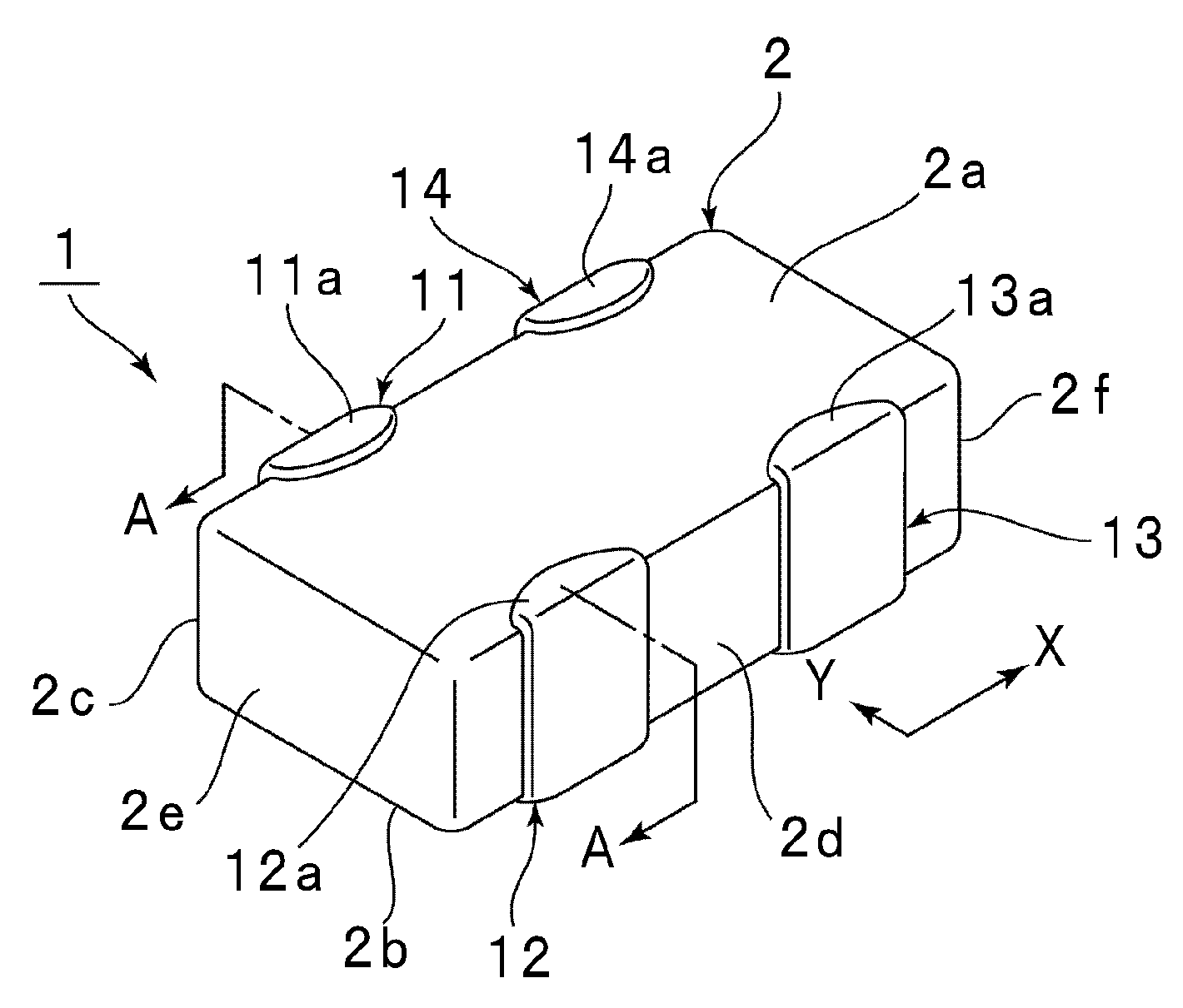
[0039]FIG. 1 is perspective view illustrating a laminated ceramic electronic component 1 according to a first preferred embodiment of the present invention. The laminated ceramic electronic component 1 of this preferred embodiment corresponds to a capacitor array.

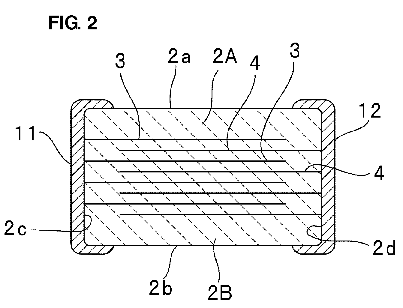
[0040]The laminated ceramic electronic component 1 includes a ceramic element body 2 formed by laminating a plurality of ceramic layers and firing the laminated ceramic layers to provide a laminated body. The ceramic element body 2 has a substantially box shape and includes a first main surface 2a, a second main surface 2b which faces the first main surface 2a, and first to fourth side surfaces 2c to 2f which are connected to the first and second main surfaces 2a and 2b. The first and second side surfaces 2c and 2d face each other, and the third and fourth side surfaces 2e and 2f face each other.

[00...


PUM

PropertyMeasurementUnit
aspect ratiosaaaaaaaaaa

Abstract

In a laminated ceramic electronic component including a ceramic element body including a plurality of effective sections, each of which constitutes a circuit element such as a laminated capacitor unit, bumps generated between the effective portions and a gap interposed between the effective portions can be made minimized. Specifically, the ceramic element body includes a first effective section including a first circuit element and a second effective section including a second circuit element. A gap is provided between the first and second effective section. Floating internal conductors are arranged in the gap at least in one of first and second external layer sections, the first external section being interposed between a first main surface and the first and second effective sections, and the second external layer section being interposed between a second main surface and the first and second effective sections.

Description

BACKGROUND OF THE INVENTION[0001]1. Field of the Invention[0002]The present invention relates to laminated ceramic electronic components such as laminated ceramic capacitors, ceramic multilayer substrates, and laminated ceramic thermistors, and particularly relates to a laminated ceramic electronic component including a ceramic element body including a plurality of effective sections which function as circuit elements, such as capacitor units, for example.[0003]2. Description of the Related Art[0004]In recent years, as electronic apparatuses become miniaturized, ceramic electronic components which are implemented on substrates of electronic apparatuses also have been miniaturized. Therefore, various array-type ceramic electronic components, each of which includes a single chip component having a plurality of functions of electronic components, have been proposed.[0005]For example, Japanese Unexamined Patent Application Publication No. 2000-331879 discloses a laminated capacitor arra...

Claims


Application Information

Patent Timeline
Patent Type & Authority Patents(United States)
IPC IPC(8): H01G4/06
CPCH01G4/012H01G4/232H01G4/30
Inventor ISHIDA, ATSUSHITANIGUCHI, TAKUMITANI, MASAKI
Owner MURATA MFG CO LTD
Why Eureka
Try Eureka