Nonvolatile memory device and method of manufacturing the same
a memory device and non-volatile technology, applied in the direction of digital storage, semiconductor/solid-state device details, instruments, etc., can solve the problems of diode itself being thermally broken down, information rewriting is difficult, and the off current required for appropriate reading cannot be maintained
- Summary
- Abstract
- Description
- Claims
- Application Information
AI Technical Summary
Benefits of technology
Problems solved by technology
Method used
Image
Examples
first embodiment
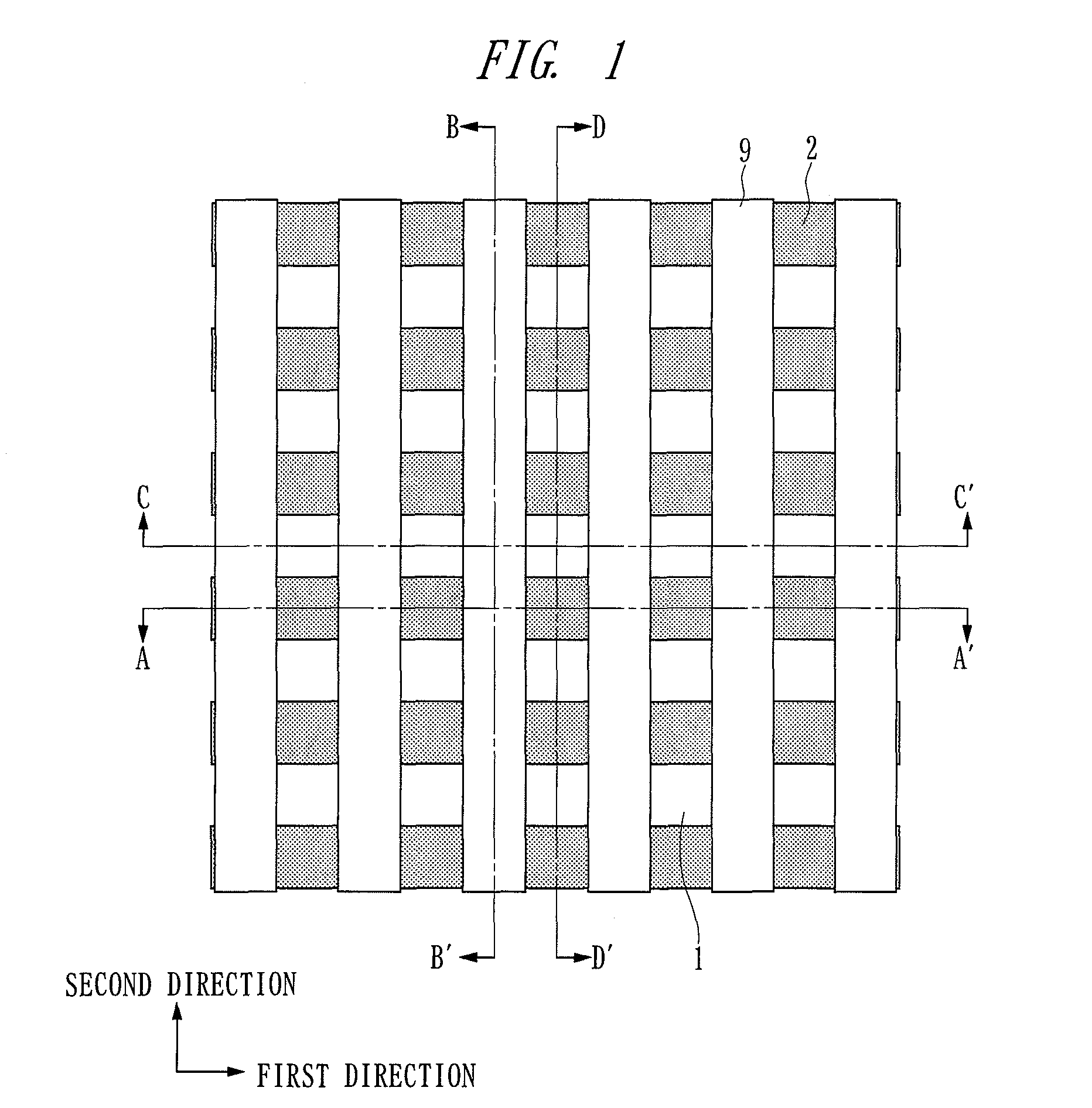
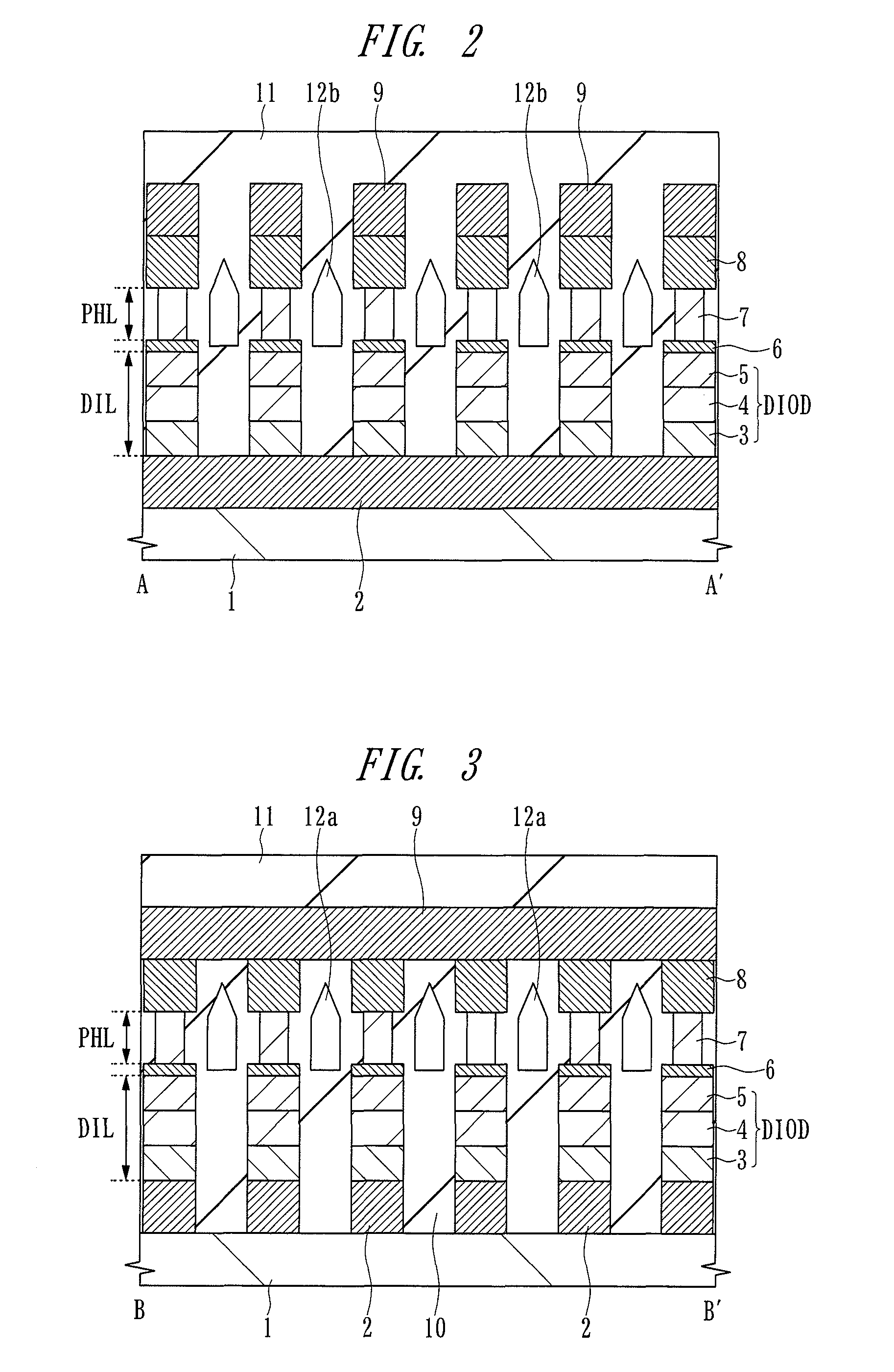
[0085]A memory matrix of a phase-change memory according to a first embodiment will be described with reference to FIG. 1 to FIG. 5. FIG. 1 is a top view of the memory matrix, FIG. 2 is a cross-sectional view of main parts of the memory matrix taken along the line A-A′ of FIG. 1, FIG. 3 is a cross-sectional view of main parts of the memory matrix taken along the line B-B′ of FIG. 1, FIG. 4 is a cross-sectional view of main parts of the memory matrix taken along the line C-C′ of FIG. 1, and FIG. 5 is a cross-sectional view of main parts of the memory matrix taken along the line D-D′ of FIG. 1. In FIG. 1, only a third metal wiring, a first metal wiring and a semiconductor substrate are illustrated for facilitating understanding of the structure of the memory matrix.
[0086]In the figures, reference numeral 1 denotes a semiconductor substrate and reference numeral 2 denotes a first metal wiring extending along a first direction. Further, reference numeral 3 denotes a first polycrystallin...
second embodiment
[0118]A memory matrix of a phase-change memory according to a second embodiment will be described with reference to FIGS. 23 to 25. FIG. 23 is a top view of the memory matrix, FIG. 24 is a cross-sectional view of main parts of the memory matrix taken along the line A-A′ of FIG. 23, and FIG. 25 is a cross-sectional view of main parts of the memory matrix taken along the line B-B′ of FIG. 23. In FIG. 23, only a third metal wiring 9, a first metal wiring 2, and a semiconductor substrate 1 are illustrated for facilitating understanding of the structure of the memory matrix. In the figures, similarly as in the first embodiment described above, reference numeral 1 denotes a semiconductor substrate and reference numeral 2 denotes a first metal wiring extending along a first direction. Further, reference numeral 3 denotes a first polycrystalline silicon film, reference numeral 4 denotes a second polycrystalline silicon film, reference numeral 5 denotes a third polycrystalline silicon film, ...
third embodiment
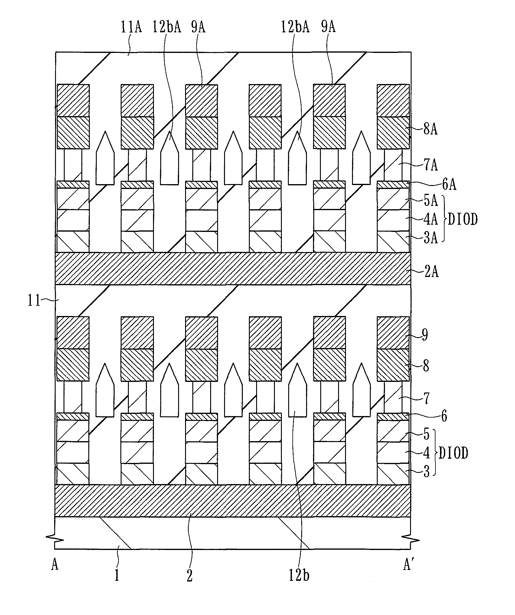
[0137]A memory matrix of a phase-change memory according to a third embodiment will be described with reference to FIGS. 38 to 40. FIG. 38 is a top view of the memory matrix, FIG. 39 is a cross-sectional view of main parts of the memory matrix taken along the line A-A′ of FIG. 38, and FIG. 40 is a cross-sectional view of main parts of the memory matrix taken along the line B-B′ of FIG. 38. In FIG. 38, only a third metal wiring, a first metal wiring, and a semiconductor substrate are illustrated for facilitating understanding of a structure of the memory matrix. In the figures, similarly as those in the first embodiment described above, reference numeral 1 denotes a semiconductor substrate and reference numeral 2 denotes a first metal wiring extending along a first direction. Further, reference numeral 3 denotes a first polycrystalline silicon film, reference numeral 4 denotes a second polycrystalline silicon film, reference numeral 5 denotes a third polycrystalline silicon film, and...
PUM
 Abstract
Description
Claims
Application Information


