
Work function engineering for eDRAM MOSFETs

a technology of work function and edram mosfet, which is applied in the field of field effect transistor (fet) fabrication, can solve problems such as information eventually fad

Active Publication Date: 2012-03-06
GLOBALFOUNDRIES U S INC
View PDF12 Cites 119 Cited by
  • Summary
  • Abstract
  • Description
  • Claims
  • Application Information

AI Technical Summary

Benefits of technology

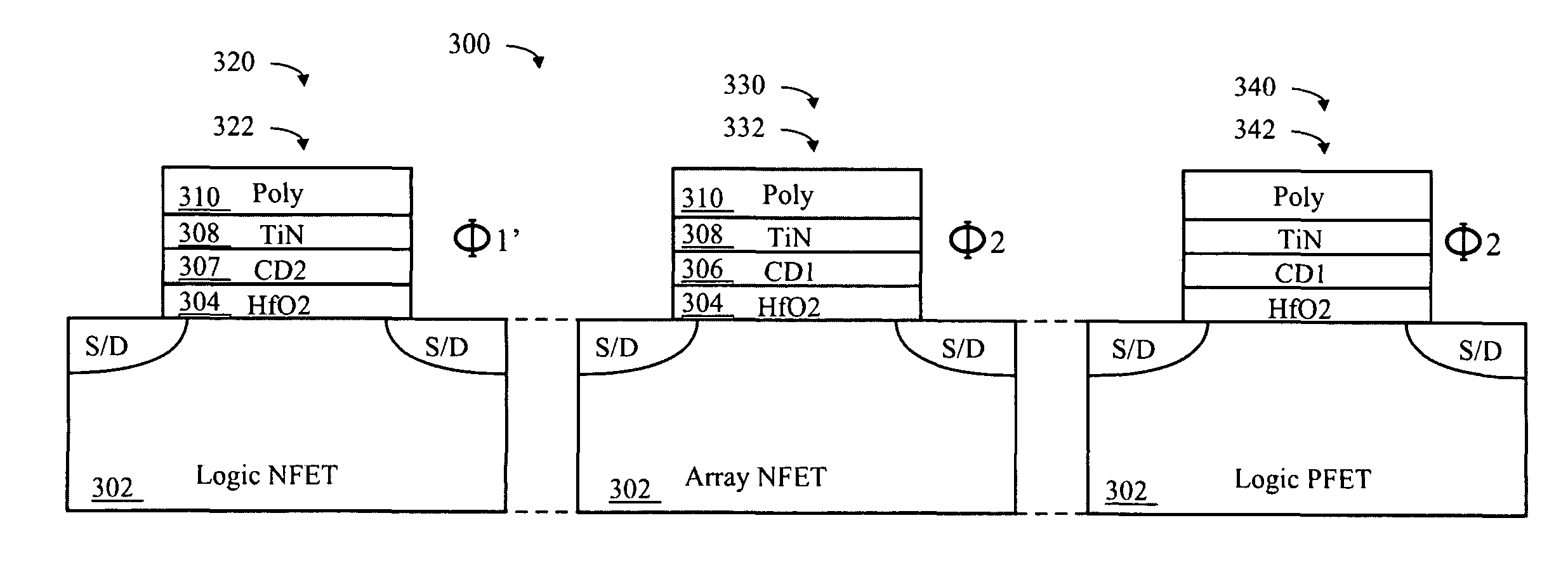
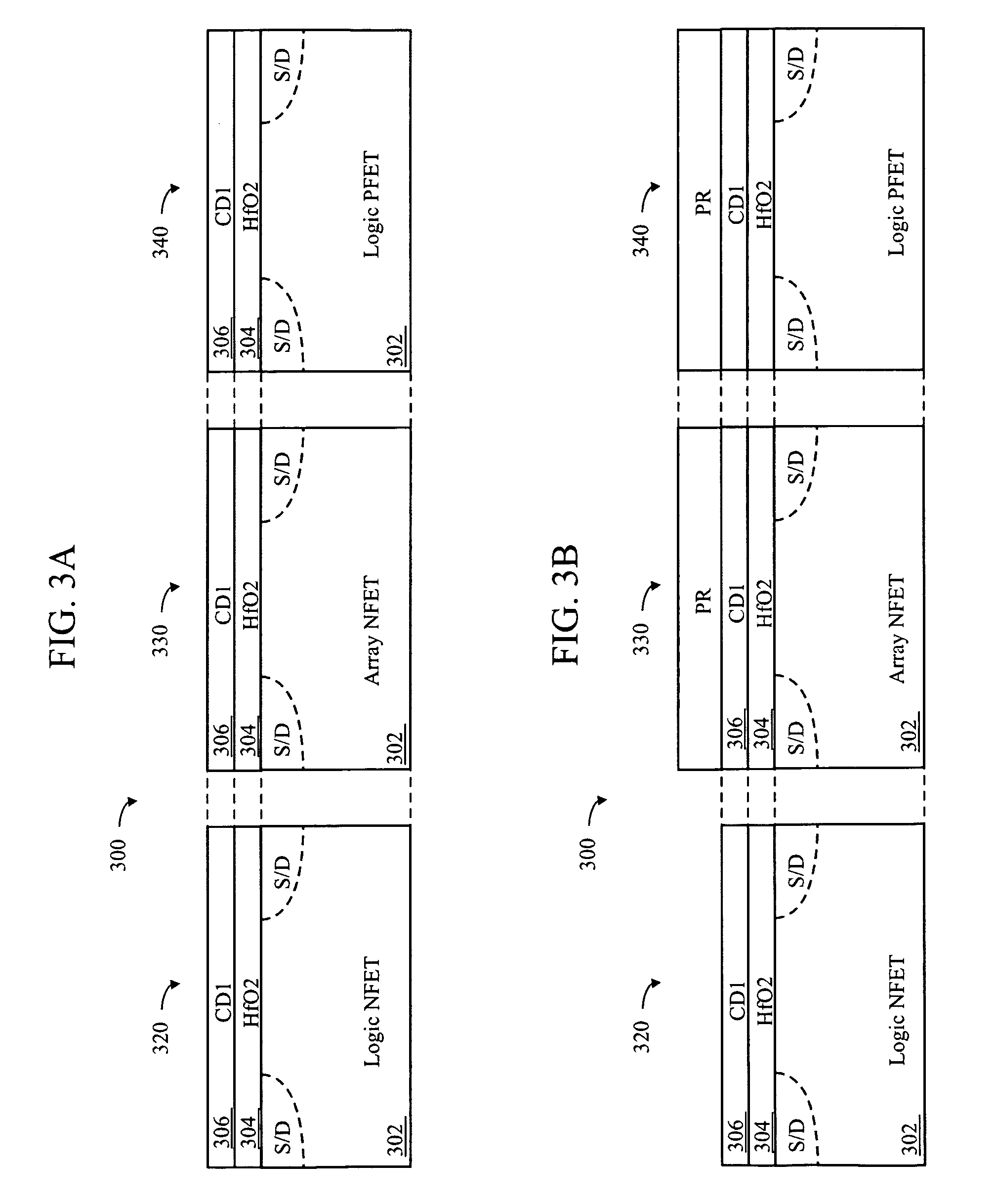
The invention relates to a method of manufacturing embedded DRAM (eDRAM) MOSFETs. The method includes depositing layers of high-K dielectric material, metal oxide, and conductive material on a semiconductor substrate, and patterning them to form gate stacks for an array NFET, a logic PFET, and a logic NFET. The technical effect of this invention is to provide a more efficient and reliable method for manufacturing eDRAM MOSFETs.

Problems solved by technology

Since real capacitors leak charge, the information eventually fades unless the capacitor charge is refreshed periodically.

Method used


Image

  • Work function engineering for eDRAM MOSFETs
  • Work function engineering for eDRAM MOSFETs
  • Work function engineering for eDRAM MOSFETs

Examples


Embodiment Construction

[0038]The leakage for EDRAM array transistor is very critical to make good retention time. Junction leakage is a critical component of the total leakage. High doping in the channel is needed for array transistor to make enough High Vt (>0.8V, logic NFET Vt is below 0.5V) to reduce the subthreshold leakage which can increase the junction leakage. In this disclosure, the gate stack with work function away from conduction band is used for the array transistor, therefore high Vt can be achieved without high channel doping. With low channel doping, the junction leakage and Vt mismatch can be reduced.

[0039]According to the invention, generally, for EDRAM, a metal oxide cap is added over the gate dielectric layer of the EDRAM array device (or “memory transistor”) to move the workfunction of the memory transistor close to the valence band edge, to increase the Vt of the EDRAM array device, with low or no channel doping. The metal oxide cap (CD1) may comprise aluminum oxide.

[0040]Therefore:[...


PUM


Abstract

Embedded DRAM MOSFETs including an array NFET having a gate stack comprising a high-K dielectric layer upon which is deposited a first metal oxide layer (CD1) then a conductive layer (TiN), and then a polysilicon layer (Poly). A logic PFET having substantially the same gate stack as the array NFET, and a logic NFET having a third gate stack comprising the high-K dielectric layer upon which is deposited the conductive layer (TiN) and then the polysilicon layer (Poly), without the first metal oxide layer (CD1) between the high-K dielectric layer and the conductive layer (TiN). The array NFET may therefore have a higher gate stack work function than the logic NFET, but substantially the same gate stack work function as the logic PFET.

Description

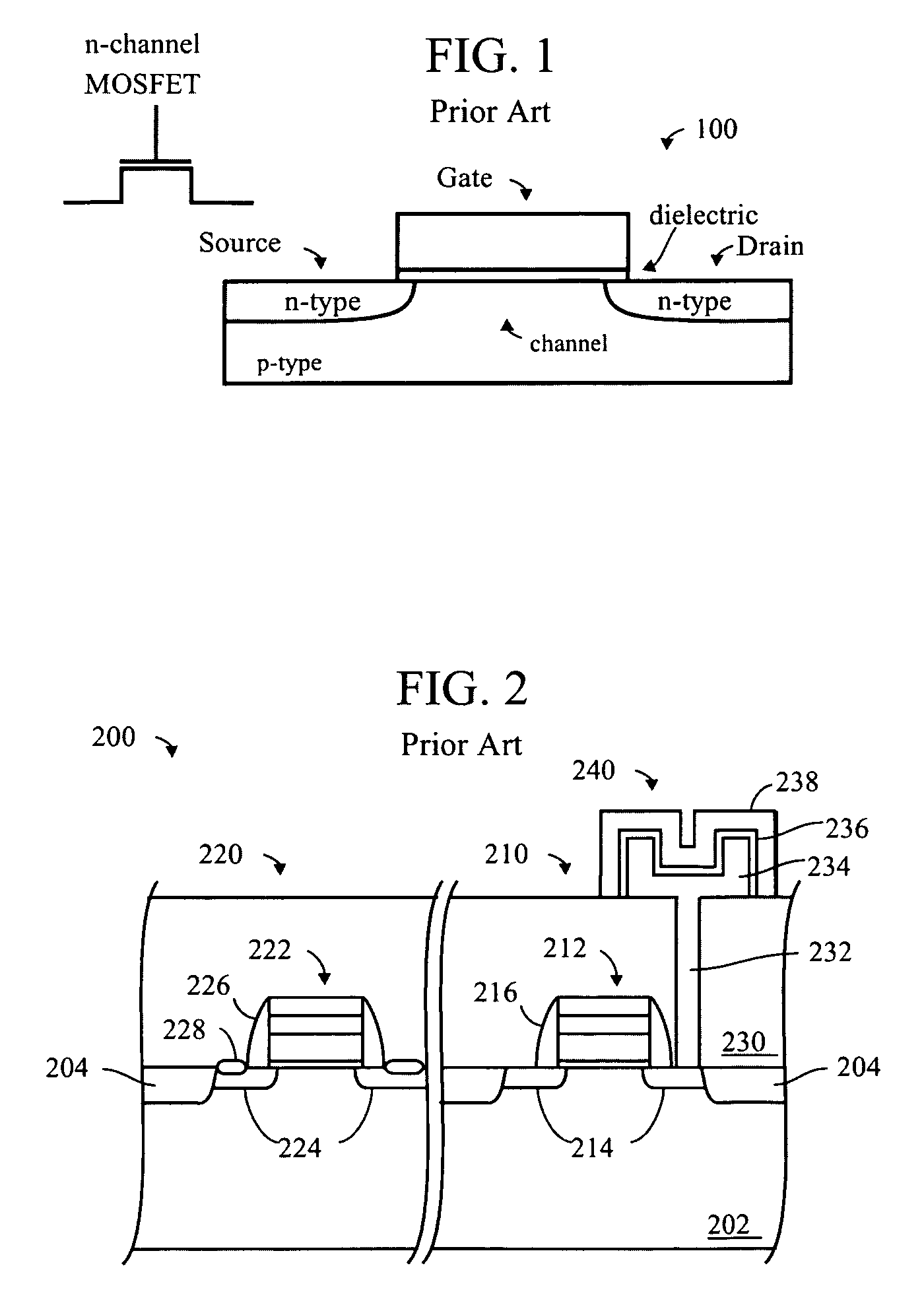
FIELD OF THE INVENTION[0001]The invention relates to semiconductor devices and, more particularly to the fabrication of field effect transistors (FETs), such as for dynamic random access memory (DRAM), such as embedded DRAM (eDRAM).BACKGROUND OF THE INVENTION[0002]The transistor is a solid state semiconductor device which can be used for amplification, switching, voltage stabilization, signal modulation and many other functions. Generally, a transistor has three terminals, and a voltage applied to a specific one of the terminals controls current flowing between the other two terminals. One type of transistor is known as the field effect transistor (FET).[0003]The terminals of a field effect transistor (FET) are commonly named source, gate and drain. In the FET, a small amount of voltage is applied to the gate (G) in order to control current flowing between the source (S) and drain (D). In FETs, the main current appears in a narrow conducting channel formed near (usually primarily un...

Claims


Application Information

Patent Timeline
Patent Type & Authority Patents(United States)
IPC IPC(8): H01L27/088H10B12/00
CPCH01L27/105H01L27/10894H01L29/4966H01L29/513H01L29/517H01L27/1052H10B12/09
Inventor CHEN, XIANGDONGHO, HERBERT L.WANG, GENG
Owner GLOBALFOUNDRIES U S INC
Learn More