Memory device and method of operation thereof

a memory device and memory technology, applied in the field of memory devices, can solve the problems of reducing the writability of memory cells of the sram device, power consumption of the device chip or chips, and power consumption of the device itself, and achieve the effect of lowering the electric potential

Active Publication Date: 2012-03-06
STMICROELECTRONICS PVT LTD
View PDF2 Cites 14 Cited by
  • Summary
  • Abstract
  • Description
  • Claims
  • Application Information

AI Technical Summary

Problems solved by technology

Due to high demands of portable devices, power consumption has become a major concern in chip design, especially in embedded memories, in particular static random access memory (SRAM).
Memory can contribute significantly to the power consumption of the chip or chips of the device.
However, in SRAM devices operated at a relatively low power supply voltage, a reduced writability of memory cells of the SRAM device can be an issue, since a voltage applied to a transistor in a memory cell may be insufficient for overcoming the threshold voltage of the transistor.
Technology scaling may increase this problem, since a reduction of critical dimensions of circuit elements of the memory devices may lead to an increase of process variation and, hence, to a broader distribution of threshold voltages of transistors in the memory device.
The reduced writability of memory cells can be a serious threat to the functionality of memory devices and thus to the yield of the manufacturing of memory devices.
However, the existing approaches can lead to an increase of the power consumption of the memory device, or may require a relatively large chip area for required circuitry, and can be unsuitable for low speed, low power applications such as medical applications.
Under low writability conditions of a memory cell, wherein the memory cell has a relatively low write voltage, this can have the consequence that the memory cell is not writeable.
If deep submicron technologies are employed for the manufacturing of a memory device, the spread of write voltages of memory cells in a memory device can be relatively high, which increases the likelihood of write failure occurring.
These issues can adversely affect the functionality of a memory device according to U.S. Pat. No. 6,934,213, in particular if it is operated at a low power supply voltage.

Method used


Image

  • Memory device and method of operation thereof
  • Memory device and method of operation thereof
  • Memory device and method of operation thereof

Examples


Embodiment Construction

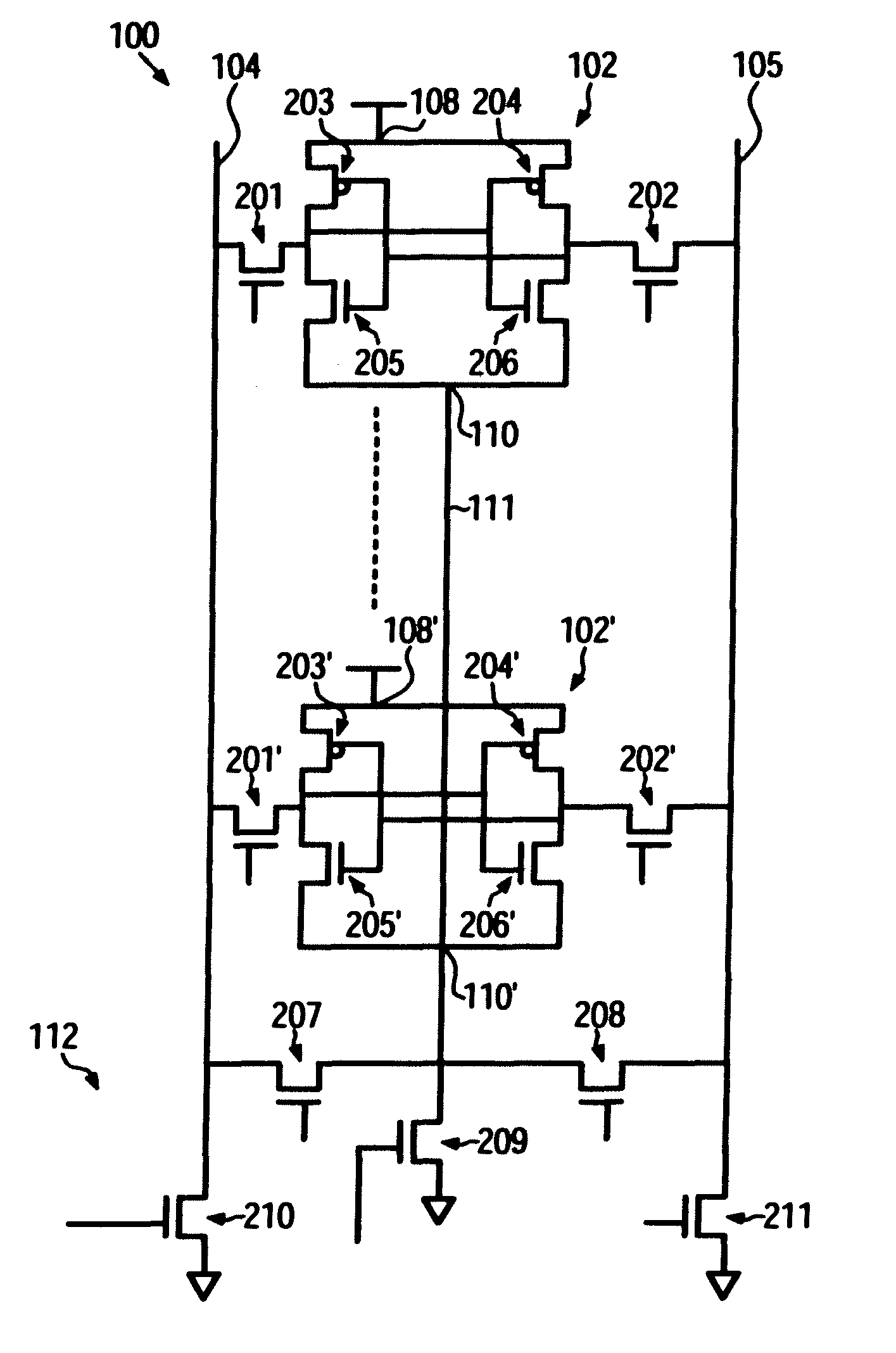
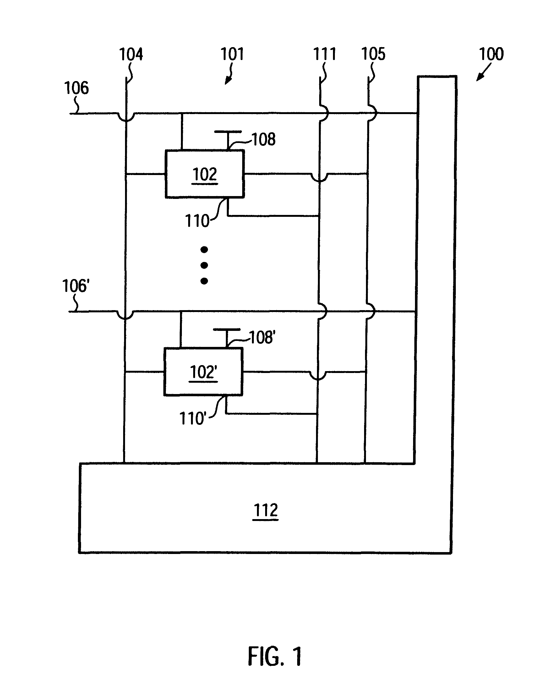
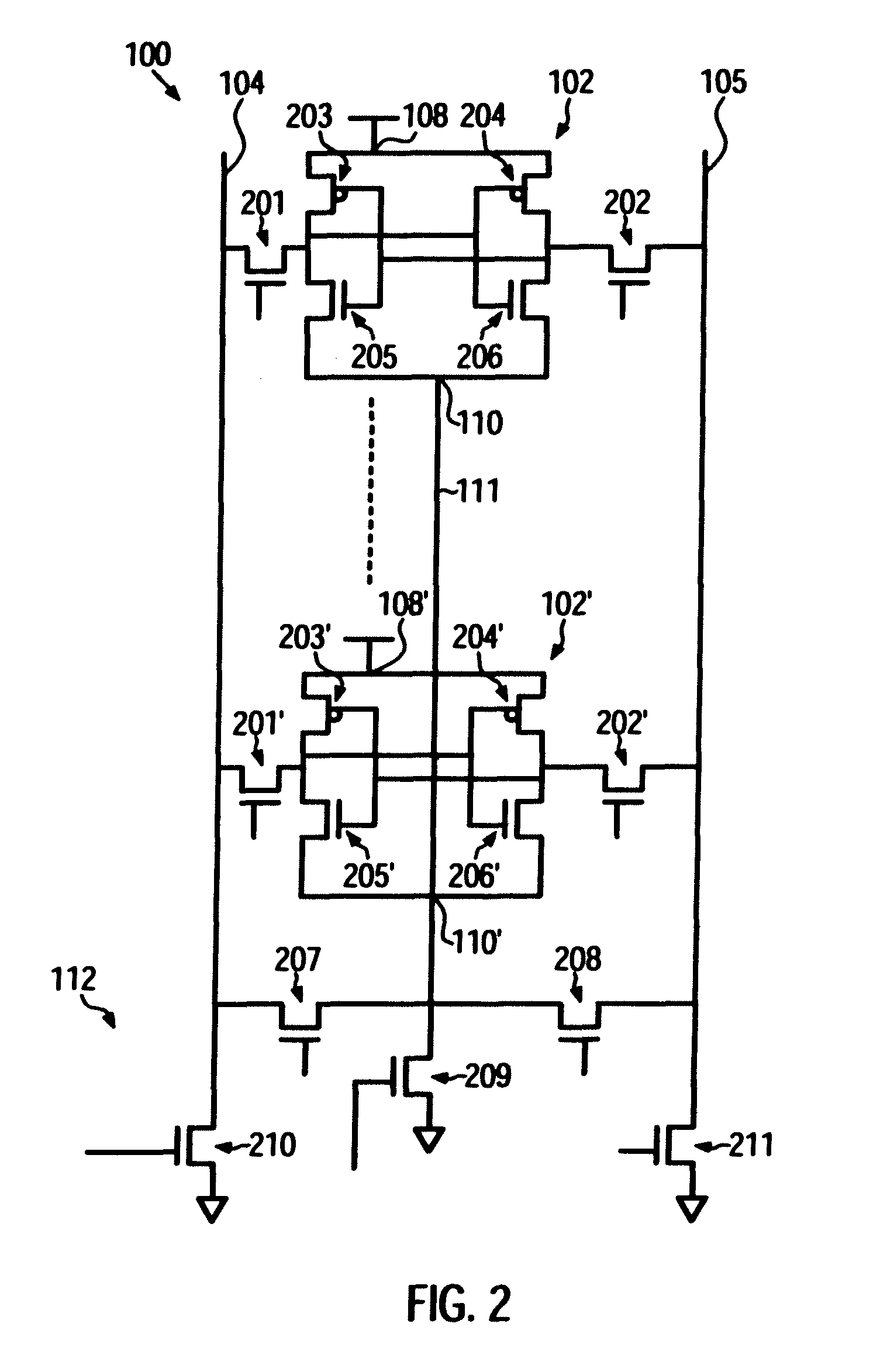
[0021]FIG. 1 shows a schematic block diagram of a memory device 100 according to an embodiment. The memory device 100 comprises a column 101 of memory cells. In addition to the column 101, the memory device 100 can comprise further columns of memory cells having a configuration corresponding to that of column 101. For simplicity, in FIG. 1, the other columns of memory cells have been omitted.

[0022]The column 101 comprises memory cells 102, 102′. Dots in FIG. 1 schematically indicate that additional memory cells can be provided between the memory cells 102, 102′. The memory cells in column 101, and in other columns of memory cells in the memory device 100, can form a matrix of memory cells.

[0023]The column 101 of memory cells can comprise a first bitline 104 and a second bitline 105 that can be complementary to the first bitline 104. Each of the memory cells 102, 102′ in column 101 can be connected to the first bitline 104 and the second bitline 105.

[0024]The present disclosure, howe...


PUM


Abstract

Memory devices and methods of operating a memory cell are disclosed in which a bitline can be grounded after charge sharing with an electrically floating ground line and before writing data to the memory cell. An electric potential of an upper power supply node of a memory cell can be lowered and an electric potential of a lower power supply node of the memory cell can be raised before writing data to the memory cell.

Description

RELATED APPLICATION[0001]The present application claims priority of India Patent Application No. 2673 / Del / 2009 filed Dec. 21, 2009, which is incorporated herein in its entirety by this reference.FIELD OF THE INVENTION[0002]The present disclosure relates to memory devices such as static memory devices (SRAM) having a relatively low power consumption.BACKGROUND OF THE INVENTION[0003]Due to high demands of portable devices, power consumption has become a major concern in chip design, especially in embedded memories, in particular static random access memory (SRAM). Memory can contribute significantly to the power consumption of the chip or chips of the device.[0004]For reducing the power consumption of a memory device, it has been proposed to reduce the power supply voltage of memory devices. A reduction of the power supply voltage can reduce the power required for charging electrically conductive lines in the memory device, in particular wordlines and bitlines, to the power supply vol...

Claims


Application Information

Patent Timeline
Patent Type & Authority Patents(United States)
IPC IPC(8): G11C7/00
CPCG11C11/412
Inventor KUMAR, ASHISHJAIN, PIYUSH
Owner STMICROELECTRONICS PVT LTD
Why Eureka
Try Eureka