Zinc oxide thin film, transparent conductive film and display device using the same

a technology of transparent conductive film and zinc oxide, which is applied in the direction of oxide conductors, non-metal conductors, applications, etc., can solve the problems of not producing a zinc oxide thin film having desired crystallinity and not producing a transparent electrode that can satisfy desired electric characteristics, and achieve excellent electric characteristics, reduce defects, and reduce the effect of manufacturing costs

Inactive Publication Date: 2012-03-20
HITACHI LTD
View PDF10 Cites 36 Cited by
  • Summary
  • Abstract
  • Description
  • Claims
  • Application Information

AI Technical Summary

Benefits of technology

[0018]The zinc oxide thin film according the present invention has desired crystallinity in which the polarity and orientation of zinc oxide are controlled on a certain substrate, and thus is a denser and less defective thin film. In addition, the transparent electrode according the present invention primarily has a zinc oxide thin film having desired crystallinity in which the polarity and orientation of zinc oxide are controlled on a certain substrate, and thus is excellent in electric characteristics.

Problems solved by technology

However, there is the problem of not fabricating a zinc oxide thin film having desired crystallinity even if the film is fabricated on a substrate in accordance with the usual method as described above.
In addition, the impossibility of fabricating a zinc oxide thin film with desired crystallinity also causes the problem of not producing a transparent electrode that can satisfy desired electric characteristics and can be used as a transparent electrode.

Method used


Image

  • Zinc oxide thin film, transparent conductive film and display device using the same
  • Zinc oxide thin film, transparent conductive film and display device using the same
  • Zinc oxide thin film, transparent conductive film and display device using the same

Examples


example 1

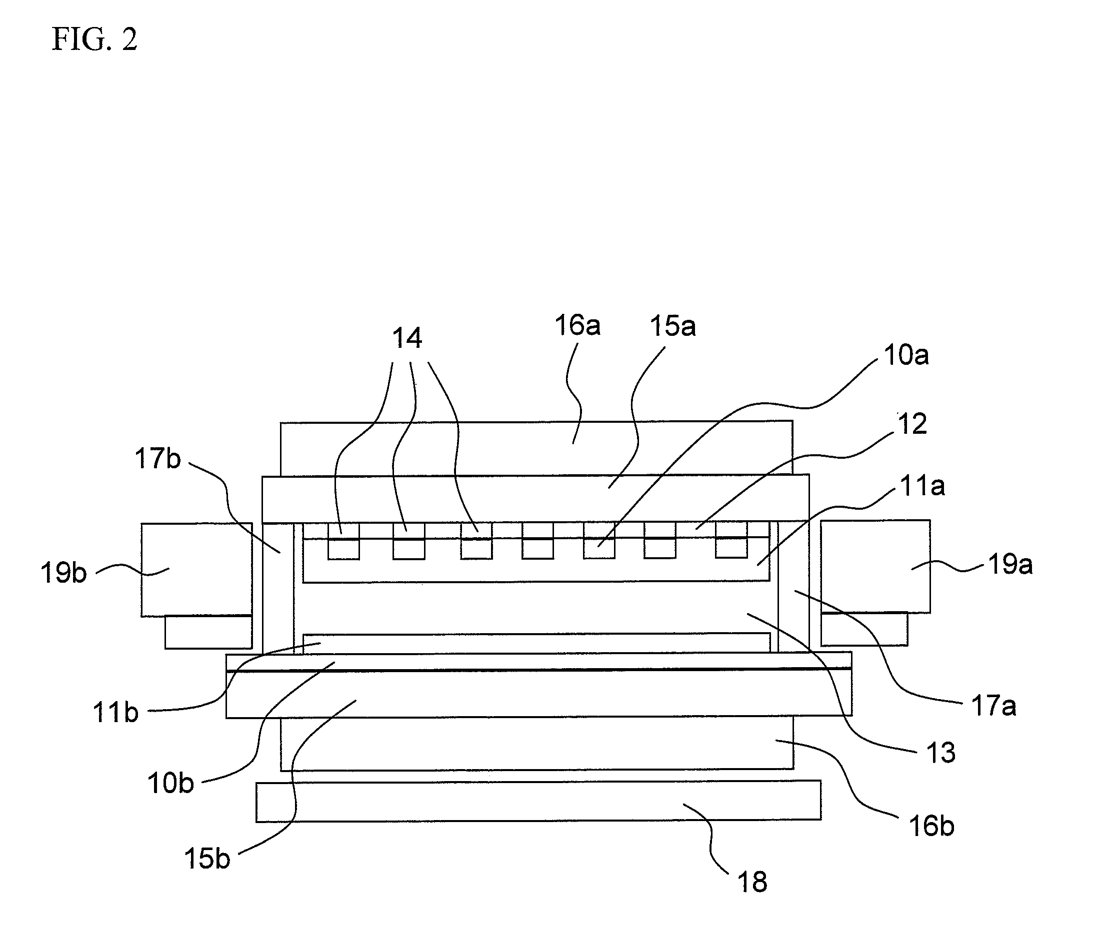
[0046]One example of a thin film fabricating process for fabricating a zinc oxide thin film of the present invention will be set forth with reference to FIG. 5. FIG. 5 indicated a constitution of vacuum equipment for thin film fabrication of zinc oxide of the present invention. This vacuum equipment for thin film fabrication includes a loading chamber 40 for carrying a substrate in the equipment, an analysis chamber 41 for analyzing a substrate surface state, a sputter chamber 42 for forming a zinc oxide thin film, a deposition chamber 43 for depositing substances except a zinc oxide thin film and a transfer chamber 44 for assigning the substrate introduced from the loading chamber 40 to the other vacuum chambers 41 to 43 without breaking vacuum, each including gate valves 45a, 45b, 45c, 45d. These five vacuum chambers are each evacuated by independent vacuum pumps that are not particularly shown. Of these, the loading chamber 40, the sputter chamber 42, deposition chamber 43 and th...

example 2

[0069]The present Example indicates the results in which a zinc oxide thin film was formed at a substrate temperature of 100° C. at the time of zinc oxide thin film fabrication. As the results, Tables 5, 6 and 7 summarize, when the film thicknesses of the zinc oxide thin film are 75 nm, 150 nm and 300 nm, respectively, physical properties of the resulting zinc oxide thin film such as c-axis orientation, polarity, transmittance, resistivity and stability of resistivity, for every temperature of sublayer and for every thickness of sublayer.

[0070]

TABLE 5ZnO film thickness: 70 nmSubstrate temperature: 100° C.Initial stage film formation: NoneThicknessStabilityTemperatureofofofsublayerorientationTransmittanceResistivityresistivitysublayer(nm)of c-axisPolarity(%)(Ωcm)(%)Room0ONP951.7E−03183temperature0.5NONP941.6E−03184 (23° C.)1NOP941.7E−031863OP931.2E−031176OP911.2E−0311810OP901.1E−0311820NOP851.7E−03183 50° C.0ONP951.6E−031860.5NONP951.7E−031831NOP951.7E−031843NOP931.6E−031836OP921.2E−...

example 3

[0075]The present Example indicates the results in which a zinc oxide thin film was formed at a substrate temperature of 200° C. at the time of zinc oxide thin film fabrication. As the results, Tables 8, 9 and 10 summarizes, when the film thicknesses of the zinc oxide thin film are 75 nm, 150 nm and 300 nm, respectively, physical properties of the resulting zinc oxide thin film such as c-axis orientation, polarity, transmittance, resistivity and stability of resistivity, for every temperature of sublayer and every thickness of sublayer.

[0076]

TABLE 8ZnO film thickness: 70 nmSubstrate temperature: 200° C.Initial stage film formation: NoneThicknessStabilityTemperatureofofofsublayerorientationTransmittanceResistivityresistivitysublayer(nm)of c-axisPolarity(%)(Ωcm)(%)Room0ONP951.2E−03179temperature0.5NONP941.2E−03182 (23° C.)1NOP941.2E−031823OP938.0E−041166OP928.1E−0411710OP898.0E−0411820NOP851.1E−03180 50° C.0ONP951.1E−031790.5NONP951.2E−031811NOP941.2E−031813OP938.2E−041166OP928.0E−041...


PUM


Abstract

A zinc oxide thin film having desired crystallinity is fabricated. The present invention provides a zinc oxide thin film which laminated on a substrate, and which is a crystalline thin film of a wurtzite form. The c-axis of the crystalline thin film is oriented in a direction substantially perpendicular to the substrate. A zinc surface of being one polar surface of the crystalline thin film in the c-axis direction is formed in the uppermost layer. In addition, the invention also provides a zinc oxide thin film which is laminated on a substrate, and which is a crystalline thin film of a wurtzite form. The zinc oxide thin film is formed on a metal thin film layer by a thin film fabricating technique.

Description

BACKGROUND OF THE INVENTION[0001]1. Field of the Invention[0002]The present invention relates to a novel zinc oxide thin film, a transparent conductive film and a display device, using the same. Specifically, the present invention relates to a thin film device that is thin, lightweight and high precision and that uses a highly efficient, long-life transparent conductive film. More specifically, the present invention relates to a liquid crystal display, a plasma display panel, a field emission display, an organic electroluminescent display, and the like.[0003]2. Description of the Related Art[0004]Recently, demand for lightweight, highly colorful, highly bright, inexpensive and small-sized flat panel display (FPD) is increasing along with the spread of various cell phones, mobile terminals, mobile computers, car navigation systems, and the like. In addition, also at home and in offices, flat panel displays such as space-saving desktop displays and wall hanging televisions are now bei...

Claims


Application Information

Patent Timeline
Patent Type & Authority Patents(United States)
IPC IPC(8): H01B1/08
CPCC23C14/022C23C14/025C23C14/086Y10S428/926
Inventor IMANISHI, YASUONISHIMURA, ETSUKO
Owner HITACHI LTD
Why Eureka
Try Eureka