
Light emitting element display device

a technology of light-emitting elements and display devices, which is applied in the direction of semiconductor devices, electrical components, electrical apparatus, etc., can solve the problems of display unevenness, degraded display quality, and increased video signal variation, and achieve high display quality

Active Publication Date: 2020-10-08
JAPAN DISPLAY INC
View PDF0 Cites 0 Cited by
  • Summary
  • Abstract
  • Description
  • Claims
  • Application Information

AI Technical Summary

Benefits of technology

This configuration stabilizes potential differences and improves display quality by reducing leakage currents and variations, enabling high-definition operation with efficient use of pixel space and enhanced driving performance.

Problems solved by technology

As a result, it is conceivable that the display quality is degraded.
In the TFT which writes the video signal into the capacitor, there is a problem in that the variation of the video signal is increased due to leakage currents, unnecessary charges, and the like when retaining the video signal and thus the display unevenness occurs.
However, in a full high definition smart phone, and the like, when high definition progresses through a control method disclosed in JP 2013-54161 A, characteristics of a transistor which writes a video signal into a capacitor are varied, thereby adversely affecting the image quality.
In addition, the driving performance of the TFT is not sufficient to supply a current to an OLED.
However, in a case where the TFT of which the channel is formed on the oxide semiconductor layer is used as a driving element for supplying a current to an OLED, there is a problem in that an operating point is greatly varied over time.
However, a leakage current amount of the transistor in which the polycrystalline semiconductor layer is used as the channel is larger than that of the transistor in which the oxide semiconductor layer is used as the channel, and thus the charge may leak from the capacitance for retaining the gate voltage of the driving transistor.

Method used


Image

  • Light emitting element display device
  • Light emitting element display device
  • Light emitting element display device

Examples


first embodiment

[0100]A configuration of a display device according to the first embodiment of the second aspect in the invention will be described with reference to FIG. 13 to FIG. 18.

Outline of Display Device

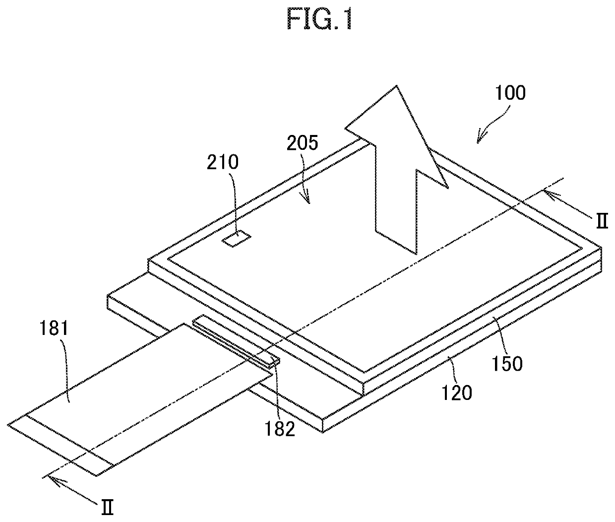
[0101]First, an outline of the display device according to the first embodiment will be described with reference to FIG. 13 and FIG. 14. FIG. 13 is a perspective view of the display device in the first embodiment according to the second aspect of the invention. In addition, FIG. 14 is a plan view of the display device in the first embodiment according to the second aspect of the invention.

[0102]As illustrated in FIG. 13 and FIG. 14, the display device in the first embodiment is provided with a light emitting element which is provided in each of a plurality of pixels, a substrate 1100 including a display area 1110 in which pixels 1180 are arranged in a matrix, a counter substrate 1200 facing the substrate 1100, a driver IC 1300 which is provided in an area to which the substrate 1100 is expose...

second embodiment

[0118]Next, a configuration of a display device according to the second embodiment of the second aspect in the invention will be described with reference to FIG. 20 to FIG. 28. Note that, portions which are not specifically mentioned are common in the second embodiment and the first embodiment.

[0119]First, a structure of the display device and a forming method thereof according to the second embodiment will be described with reference to FIG. 20 to FIG. 24. Similar to FIG. 16 to FIG. 19, FIG. 20 to FIG. 24 are perspective plan views when viewed from the display area side of the display device, and illustrate an area 2×2 pixels arranged in the vertical and horizontal directions.

[0120]FIG. 20 illustrates a state in which a LIPS layer 521 and an electrode layer 531 are formed on the same insulating layer. Here, the electrode layer 531 may be obtained by disposing the same material as that of the LIPS layer 521 on the same insulating layer, then performing an ion implantation process th...

modification 1

[0132]Next, Modification 1 of the second embodiment will be described with reference to FIG. 27. In Modification 1, it is found that the electrode layer 532 and the electrode layer 533 are formed to be extended to an area Cl in which the electrode layer 532 and the electrode layer 533 overlap the power line 563 disposed on the right side of the pixel. In this way, when forming an area, in which the power line 563 and the electrode layers 531, 532, and 533 overlap with each other, on the lower side of the power line 563, it is possible to secure a large area in which the capacitor is formed as compared with the second embodiment. Note that, as an application example of Modification 1, it is possible to form an area in which the electrode layers 531, 532, and 533 overlap the signal line 562 on the left side of the pixel without overlapping the power line 563 on the right side of the pixel.


PUM

PropertyMeasurementUnit
lengthaaaaaaaaaa

Abstract

A display device includes two or more transistors in one pixel, and the two or more transistors include a first transistor of which a channel semiconductor layer is polycrystalline silicon, and a second transistor of which a channel semiconductor layer is an oxide semiconductor.

Description

CROSS-REFERENCE TO RELATED APPLICATION[0001]This application is a continuation-in-part of U.S. patent application Ser. No. 14 / 602,909, filed on Jan. 22, 2015, which claims priority from Japanese application JP 2014-012823 filed on Jan. 27, 2014, the entire contents of which are hereby incorporated by reference into this application.BACKGROUND OF THE INVENTION1. Field of the Invention[0002]The present invention relates to a light emitting element display device.2. Description of the Related Art[0003]In recent years, light emitting element display devices using self-luminous bodies such as organic light emitting diodes (OLED) have been put into practical use. As compared with the related art liquid crystal display device, because the light emitting element display devices including an organic EL (Electroluminescent) display device using the OLED use the self-luminous bodies, the light emitting element display device not only is excellent in visibility and response speed, but also requ...

Claims


Application Information

Patent Timeline
Patent Type & Authority Applications(United States)
IPC IPC(8): H01L27/32H01L29/786H01L29/66H01L29/16H01L29/04H01L29/24H01L27/12
CPCH01L27/1225H01L27/3272H05K999/99H01L29/04H01L27/1222H01L27/3262H01L29/66757H01L29/7869H01L27/3265H01L27/3276H01L29/66969H01L29/24H01L29/78675H01L29/16H01L27/1251H01L27/1255H01L27/1229H10K59/351H10K59/1213H10K59/126H10K59/1216H10K59/131
Inventor SATO, TOSHIHIRO
Owner JAPAN DISPLAY INC
Learn More