Gate drive apparatus

a gate drive and circuit technology, applied in the direction of oscillator generators, electronic switching, pulse techniques, etc., can solve the problems of large variance of loss attributed to mirror voltage variance, affecting the speed of switching devices, and affecting the effect of switching speed

Active Publication Date: 2012-03-20
MITSUBISHI ELECTRIC CORP
View PDF15 Cites 19 Cited by
  • Summary
  • Abstract
  • Description
  • Claims
  • Application Information

AI Technical Summary

Benefits of technology

[0024]This invention has been made in order to solve the problems as stated above, and it has for its object to obtain a gate drive apparatus which can suppress the variance of switching speeds attributed to the variances of threshold voltages and mirror voltages in a plurality of switching devices to be driven by the gate drive apparatus, and which can minimize the variance of losses.
[0027]This invention brings forth remarkable advantages not existing in the prior art, as follows: A shift period in a gate drive mode is driven by the constant-current output, whereby the variance of the shift period attributed to the variances of a gate threshold voltage and a mirror voltage in the switching device can be minimized, and the variances of a switching speed and a switching loss can be sharply suppressed. Further, in the switching device of voltage drive type having a gate structure of MOS type, constant-current drive is switched to constant-voltage drive, whereby the switching device can be driven without spoiling the reliability of the gate oxide film thereof.

Problems solved by technology

Such a prior-art gate drive apparatus has had the problem that a time in which the switching device shifts from OFF to ON varies greatly, depending upon the individual characteristics of elements.
Accordingly, the variance of the loss attributed to the variance of the mirror voltage tends to become large.
Incidentally, the situation of an OFF shift is the same, and a similar problem is posed.

Method used


Image

  • Gate drive apparatus
  • Gate drive apparatus
  • Gate drive apparatus

Examples


first embodiment

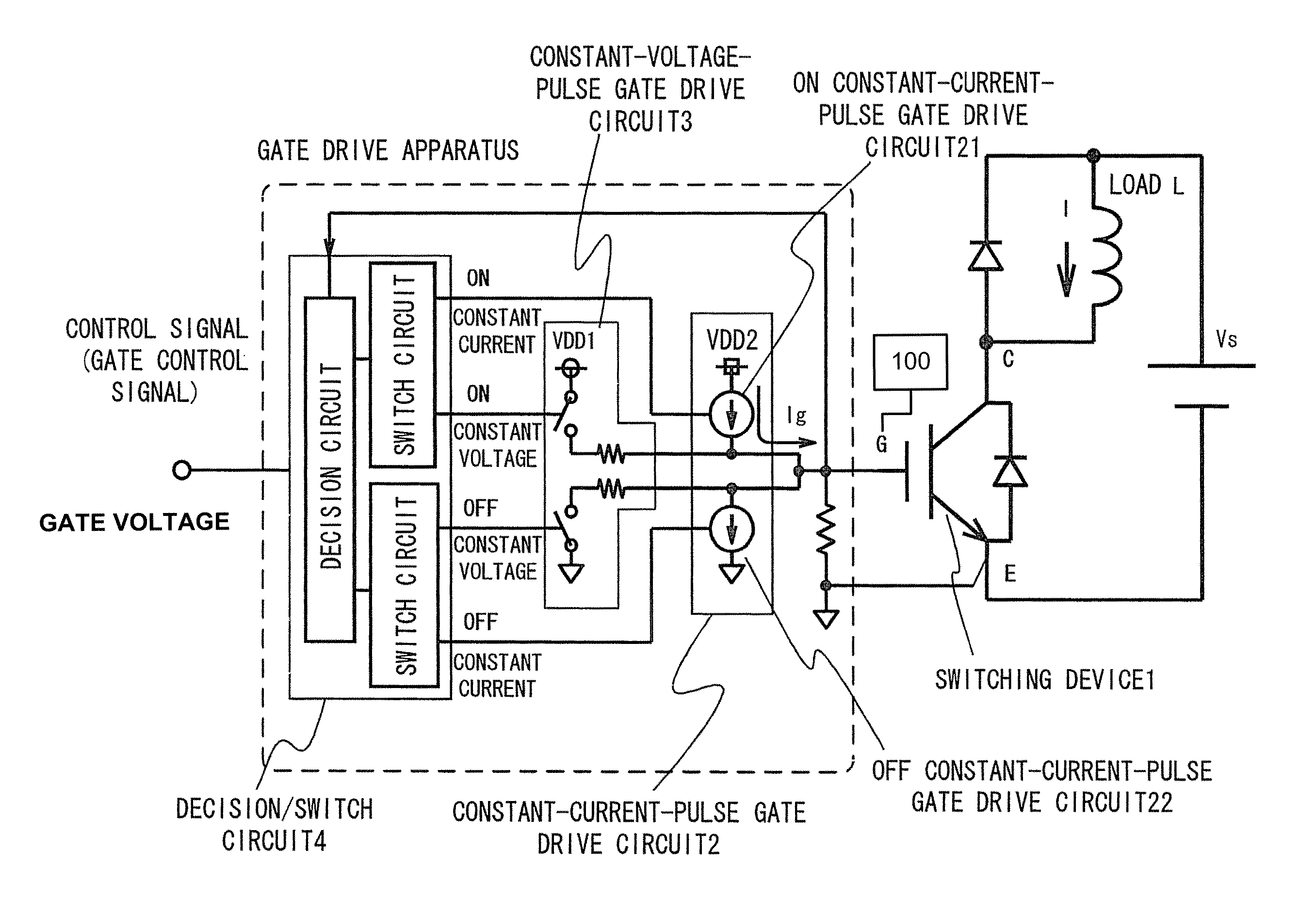
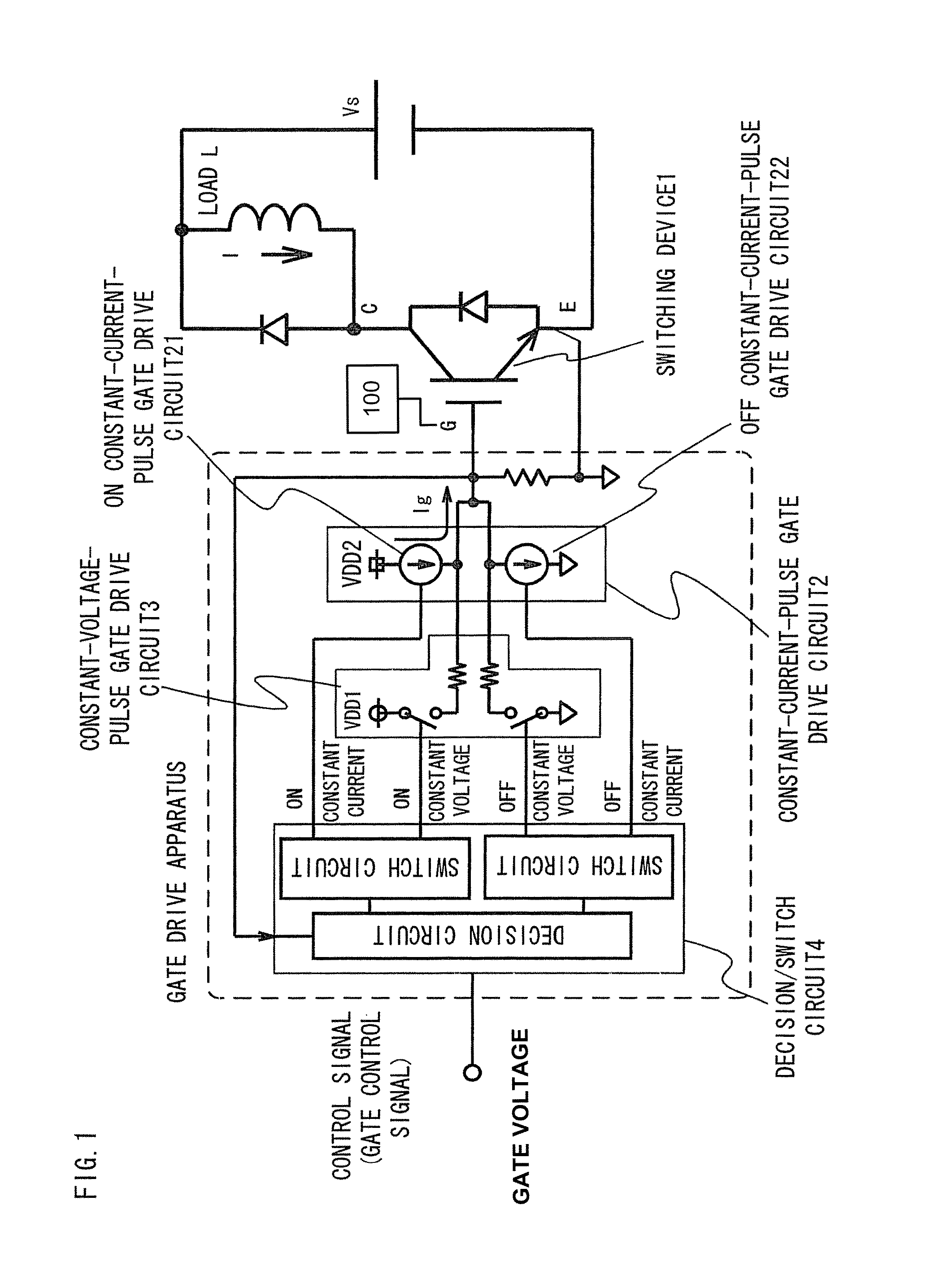
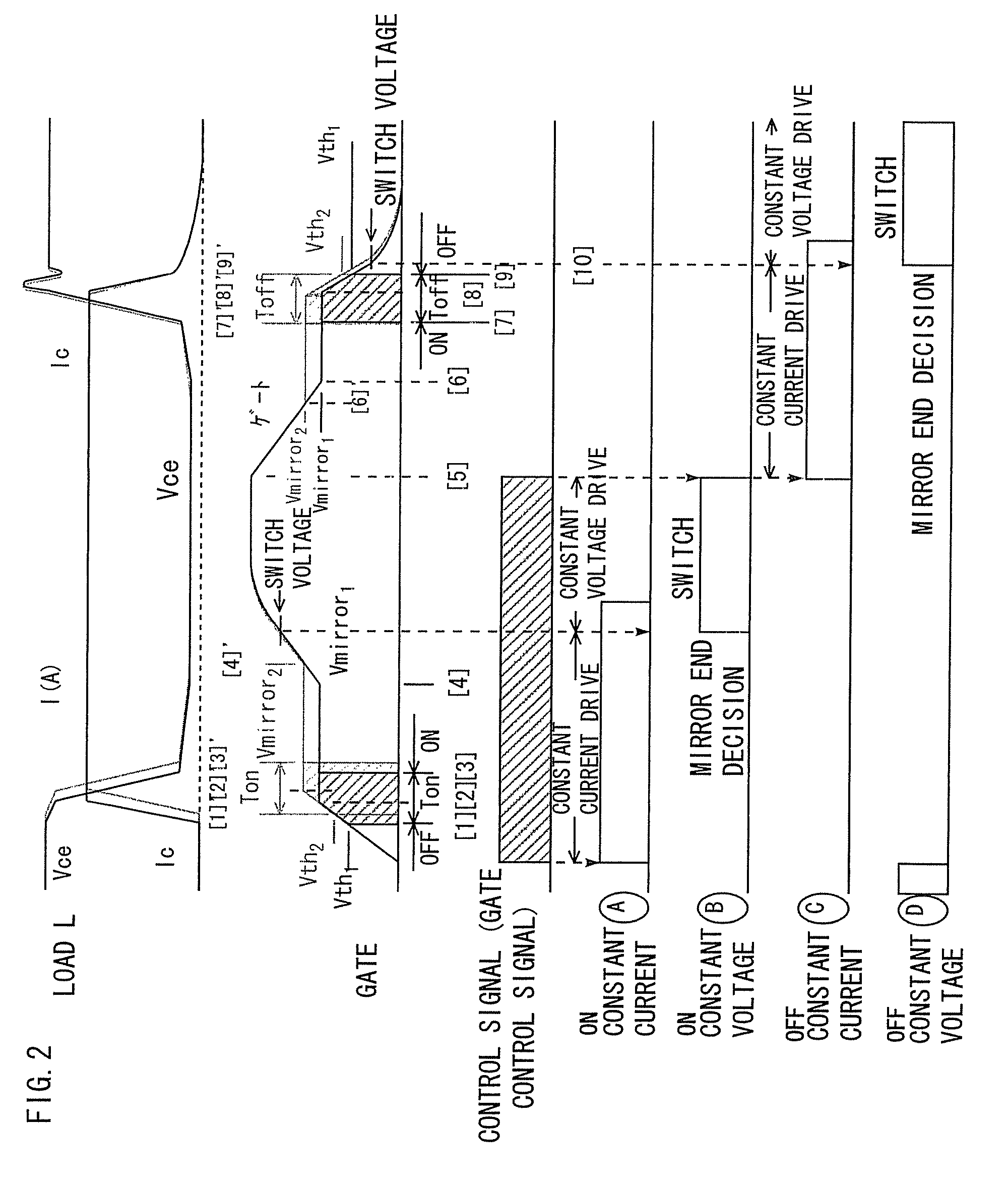
[0057]FIG. 1 is a general configurational diagram of a gate drive apparatus according to Embodiment 1 of the present invention. The output of a constant-current-pulse gate drive circuit 2 is connected to the gate of a switching device (IGBT) 1, and the output of a constant-voltage-pulse gate drive circuit 3 is further connected thereto.

[0058]A decision / switch circuit 4 receives, as inputs, a control signal (gate control signal) and the gate voltage of the switching device 1 via a gate voltage detection circuit 100. The decision / switch circuit 4 outputs and connects the control signal of ON constant current / OFF constant current to the constant-current-pulse gate drive circuit 2, and the control signal of ON constant voltage / OFF constant voltage to the constant-voltage-pulse gate drive circuit 3.

[0059]Here, the voltage VDD2 of a control power source used for the constant-current-pulse gate drive circuit 2 is set higher than the voltage VDD1 of a control power source for the constant-v...

second embodiment

[0145]In Embodiment 1, in a case where the switching from the constant current drive to the constant voltage drive needs to be performed at a high speed and where (VDD2>recommended gate voltage of the IGBT) is set on account of the response delays of the decision / switch circuit 4 and the constant-current-pulse gate drive circuit 2, the overvoltage is applied to the gate of the IGBT 1. It is accordingly apprehended that the reliability of the gate oxide film will degrade, and that the gate breakdown will be induced in the worst case. Therefore, a voltage limitation circuit 5 shown in FIG. 16 is mounted between the ON constant-current-pulse gate drive circuit 21 and the gate terminal of the IGBT 1.

[0146]The voltage limitation circuit 5 observes the gate signal at the output end thereof, and it turns OFF a high-speed cutoff element when the gate signal has become, at least, a prescribed voltage. Incidentally, the voltage limitation circuit 5 may well be controlled so as to continue a c...

third embodiment

[0153]As already stated, in the constant-current-pulse gate drive circuit 21 for use in Embodiment 1, the variance of the voltage VEB of the transistor Q1 and the temperature characteristic, for example, can form causes for the constant-current variance of the constant-current-pulse gate drive circuit 2.

[0154]Embodiment 3 suppresses the characteristic fluctuations of the transistor Q1 and the like semiconductor devices themselves constituting the constant-current-pulse gate drive circuit 21. For this purpose, as shown in FIGS. 19 and 20, the transistor Q1 and a constituent D1 (or Q1″) being a compensating semiconductor device are configured under the same conditions within an identical IC chip.

[0155]The transistor Q1 and the diode D1 or the transistor Q1″ are manufactured under the same conditions in the identical IC or chip, whereby the transistor Q1 exhibits a variance characteristic in which the variance direction of the voltage VEB agrees (when the voltage VEB increases, a volta...


PUM


Abstract

A gate drive apparatus including a constant-current-pulse gate drive circuit which creates a gate signal for a switching device as a constant-current output, a constant-voltage-pulse gate drive circuit which creates the gate signal as a constant-voltage output, and a decision / switch circuit which switches the operation of the constant-current-pulse gate drive circuit and the operation of the constant-voltage-pulse gate drive circuit. The variance of switching speeds attributed to the variances of threshold voltages and mirror voltages in a plurality of switching devices which are driven by the gate drive apparatus can be suppressed, and the variance of losses can be minimized.

Description

BACKGROUND OF THE INVENTION[0001]1. Field of the Invention[0002]This invention relates to a gate drive circuit for use in a switching device of voltage drive type, such as IGBT or FET.[0003]2. Description of the Background Art[0004]In a conventional switching device, its gate is driven through a gate resistance by a drive IC or a drive circuit connected to a gate power source (refer to, for example, Patent Document 1).[0005]Patent Document 1: JP-A-8-33315 (Sectors [0008] to [0011] and FIG. 6)[0006]Such a prior-art gate drive apparatus has had the problem that a time in which the switching device shifts from OFF to ON varies greatly, depending upon the individual characteristics of elements.[0007]Now, the variance of the ON shift time in a turn-ON period will be explained in detail by taking an IGBT as an example and together with the operation thereof, in conjunction with FIGS. 27 and 28. Incidentally, it is assumed that a load L is an inductive load, and that a current I (A) is fly...

Claims


Application Information

Patent Timeline
Patent Type & Authority Patents(United States)
IPC IPC(8): H03K17/04
CPCH03K17/0406H03K17/168H03K17/08128H03K17/063H03K17/163H03K17/00
Inventor TSUNODA, YOSHIKAZUOKUDA, TATSUYAFUKU, MASARU
Owner MITSUBISHI ELECTRIC CORP
Why Eureka
Try Eureka