Large scale MOCVD system for thin film photovoltaic devices

a photovoltaic device and mocvd technology, applied in the field of photovoltaic techniques, can solve problems such as techniques in the past, and achieve the effects of high quality, enhanced uniformity of deposited film, and cost-effectiveness

Inactive Publication Date: 2012-03-27
CM MFG
View PDF93 Cites 49 Cited by
  • Summary
  • Abstract
  • Description
  • Claims
  • Application Information

AI Technical Summary

Benefits of technology

[0009]It is to be appreciated that the invention provides numerous benefits over conventional techniques. Among other things, the systems and processes of the present invention are compatible, but scaled from conventional systems, which allow cost effective implementation of conventional chemical vapor deposition into applications for depositing thin films substantially uniformly on large surface area of glass substrates with various dimensions up to 165 cm. In various embodiments, the apparatus and structures associated with the chemical liquid delivery, doping gas delivery, and vapor generation, vapor mixing to form precursor, precursor vapor delivery, temperature control for both precursor and substrate, and the large sized substrate handling with structure integrity have been disclosed to provide various advantages over the conventional techniques. In one or more embodiments, the precursor vapor delivery is implemented in a lid member configured to distribute the vapor substantially uniform and steady in a downward flow over the substrate surface. The deposition chamber is added an interior shield structure configured to cover almost all interior surfaces except a number of channels in a frame structure around all outer side regions of the heater plates above a base member. The channels guide the downward-flow vapor that flows laterally across the surface of the substrates and over the outer side regions. The downstream flow further is guided to pass through the shield structure towards an exit port built below the heater plates in a central region of the base member structure, where the exit port is coupled to a pump module via a valve stack to remove the vapor residue. This flow pattern substantially enhances the uniformity of the deposited film on the substrates with large form factor of 165×65 cm or the like. For example, high quality and low cost large scale manufacture of thin film photovoltaic panels directly on extra large glass substrates are achieved with overall efficiency over 11%. There are other benefits as well.

Problems solved by technology

In the process of manufacturing CIS and / or CIGS thin films, there are various manufacturing challenges, such as scaling up the manufacturing to large substrate panels while maintaining structure integrity of the substrate materials, ensuring uniformity and granularity of the thin film material, etc.
While conventional techniques in the past have addressed some of these issues, they are often inadequate.

Method used


Image

  • Large scale MOCVD system for thin film photovoltaic devices
  • Large scale MOCVD system for thin film photovoltaic devices
  • Large scale MOCVD system for thin film photovoltaic devices

Examples


Embodiment Construction

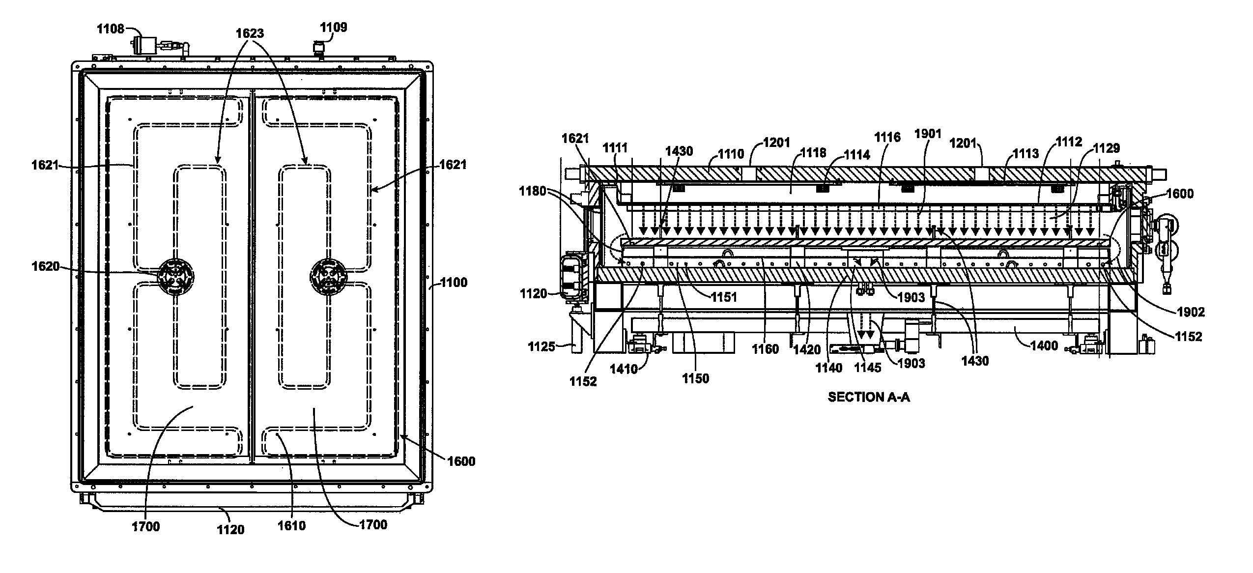
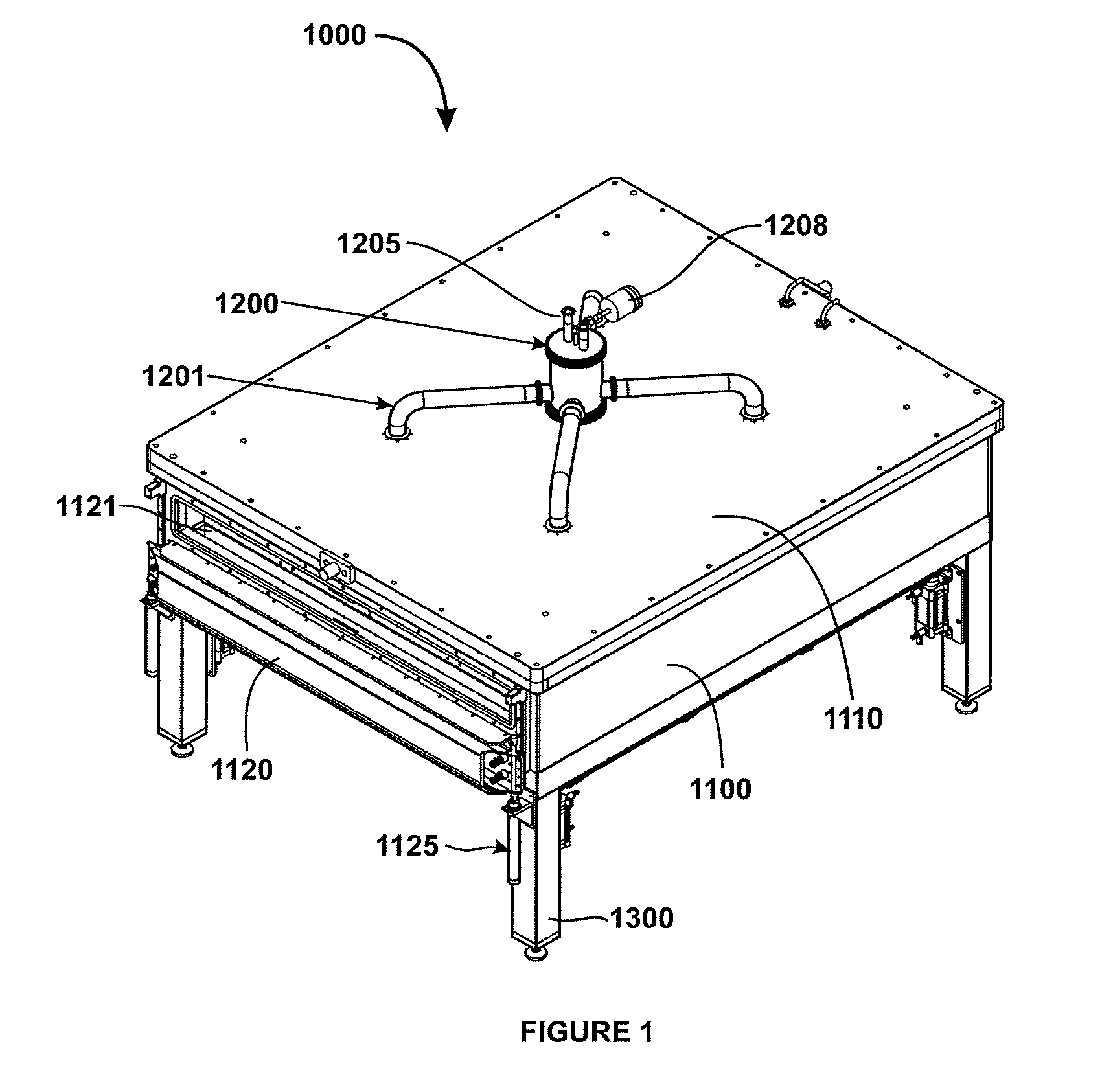
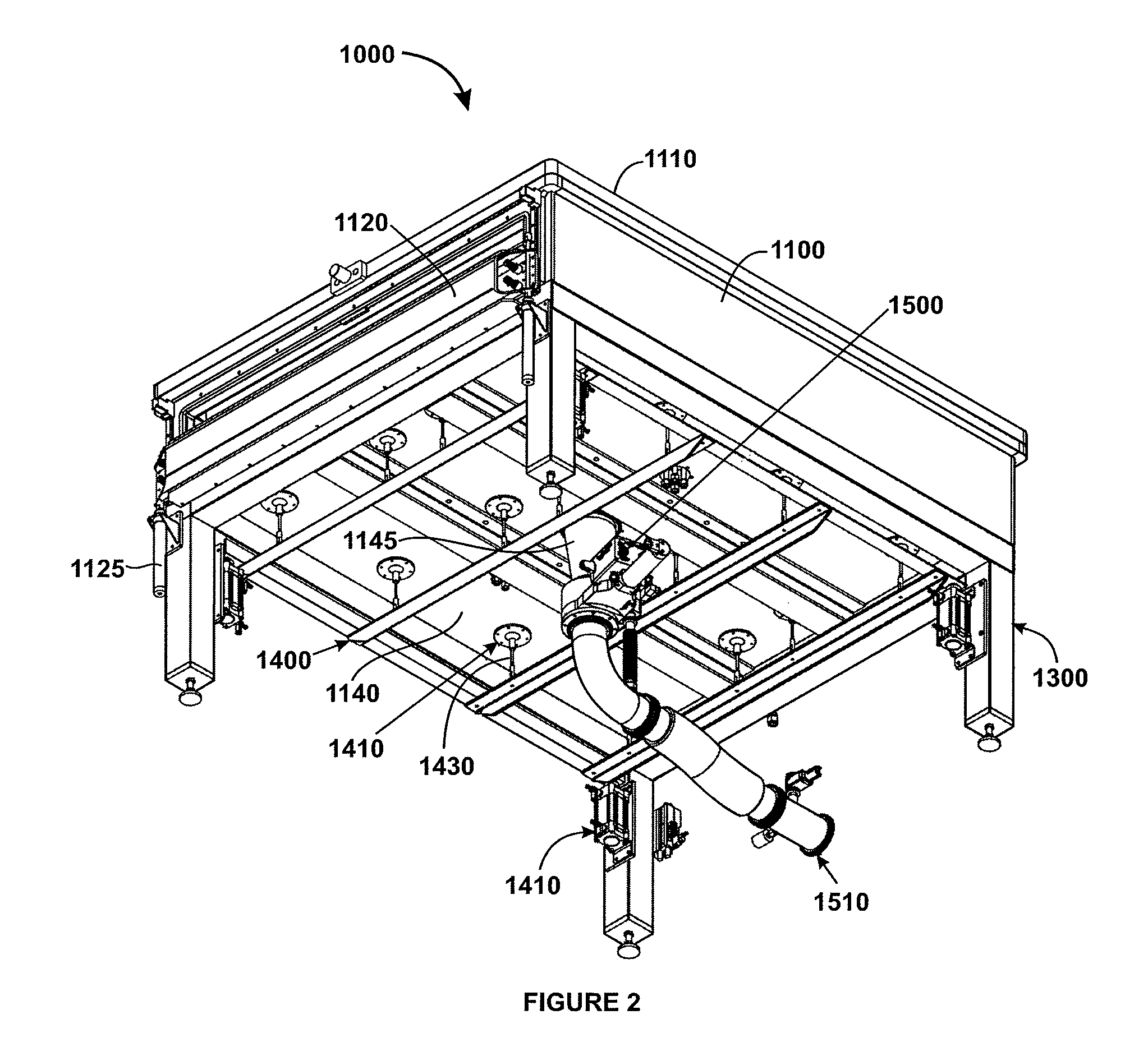
[0025]FIG. 1 is a perspective view of a metal-organic chemical vapor deposition process chamber according to an embodiment of the present invention. As shown, a process chamber 1000 is provided for fabricating thin film photovoltaic devices on substrate panels using chemical vapor deposition technique, although it can be applied for many other devices on substrate panels with large form factors. The process chamber 1000 includes a deposition chamber 1100 and a mixing chamber 1200. The mixing chamber 1200 is configured to mix several gases to form a mixed gas or vapor material required for performing vapor deposition in the deposition chamber 1100. The mixing chamber 1200 is disposed above the deposition chamber 1100, coupling each other via several pipes 1201. The deposition chamber 1100 has a substantially rectangular shape and is supported at its four corners by a support member 1300. The chamber is designed to have a sufficiently large lateral dimension capable of holding one or ...


PUM

PropertyMeasurementUnit
sizeaaaaaaaaaa
sizesaaaaaaaaaa
sizesaaaaaaaaaa

Abstract

An apparatus for fabricating thin films on substrate panels includes a deposition chamber enclosed by sidewalls, a lid, and a base. The apparatus includes a mixing chamber disposed above the lid and configured to receive vapor species and form a mixed vapor. The mixing chamber is coupled with the deposition chamber via inlets through the lid, including a diffuser plate. Two heater plates disposed side by side on the base supporting and heating two substrates.

Description

CROSS-REFERENCE TO RELATED APPLICATIONS[0001]This application claims priority to U.S. Provisional Application No. 61 / 318,750, filed Mar. 29, 2010, commonly assigned, and hereby incorporated by reference in its entirety herein for all purpose.BACKGROUND OF THE INVENTION[0002]This invention relates to photovoltaic techniques, and in particular to a large scale system and method for manufacturing thin film photovoltaic devices using copper indium diselenide species (CIS), copper indium gallium diselenide species (CIGS), as well as other materials. The invention can be applied to implement a Metal-Organic Chemical Vapor Deposition (MOCVD) system for depositing metal oxide materials for manufacturing thin film photovoltaic devices on large scale substrate panels.[0003]In the process of manufacturing CIS and / or CIGS thin films, there are various manufacturing challenges, such as scaling up the manufacturing to large substrate panels while maintaining structure integrity of the substrate m...

Claims


Application Information

Patent Timeline
Patent Type & Authority Patents(United States)
IPC IPC(8): H01L21/00
CPCC23C16/45512C23C16/45565C23C16/45572C23C16/46C23C16/54H01L31/18C23C16/4586Y10T29/413
Inventor WIETING, ROBERT D.DOERING, KENNETH B.SCHMITZBURGER, JURG
Owner CM MFG
Why Eureka
Try Eureka