Nitride crystal with removable surface layer and methods of manufacture

a technology of nitride crystals and surface layers, applied in the field of crystal processing, can solve the problems of additional defects, thermal expansion mismatch, impurities, tilt boundaries, etc., and achieve the effect of simple and cost-effectiv

Active Publication Date: 2012-04-03
SLT TECH
View PDF122 Cites 114 Cited by
  • Summary
  • Abstract
  • Description
  • Claims
  • Application Information

AI Technical Summary

Benefits of technology

[0013]In an alternative specific embodiment, the present invention provides a method of making a nitride crystal with a removable surface layer. The method includes providing a high quality nitride base crystal, comprising a nitrogen species and having a surface dislocation density below 105 cm−2. In a specific embodiment, the high quality nitride base crystal comprises a surface region and forming a release layer overlying the surface region. The release layer has an optical absorption coefficient greater than 1000 cm−1 at at least one wavelength where the high quality nitride base crystal is substantially transparent, with an optical absorption coefficient less than 50 cm−1. The method includes forming a high quality epitaxial layer comprising a nitrogen species and having a surface dislocation density below 105 cm−2 overlying the release layer.
[0016]Benefits are achieved over pre-existing techniques using the present invention. In particular, the present invention provides a method and device using a release layer for manufacture of high quality films such as such as GaN, AlN, InN, InGaN, and AlInGaN and others. In a specific embodiment, the present method and device use techniques that are relatively simple and cost effective. Depending upon the embodiment, the present apparatus and method can be manufactured using conventional materials and / or methods according to one of ordinary skill in the art. Depending upon the embodiment, one or more of these benefits may be achieved. These and other benefits may be described throughout the present specification and more particularly below.

Problems solved by technology

However, the quality and reliability of these devices is compromised by very high defect levels, particularly threading dislocations, grain boundaries, and strain in semiconductor layers of the devices.
Additional defects can arise from thermal expansion mismatch, impurities, and tilt boundaries, depending on the details of the growth method of the layers.
The presence of defects has a deleterious effect on epitaxially-grown layers, compromising electronic device performance and requiring complex, tedious fabrication steps to reduce the concentration and / or impact of the defects.
It is possible to reduce the surface dislocation density by methods that are known in the art, such as epitaxial lateral overgrowth, but these methods generally are not able to produce layers with a dislocation density below about 105 cm−2 over the entire surface.
In addition, the presence of voids or porosity may be deleterious to material quality in relatively thin epitaxial layers.
These methods do not provide a natural endpoint, and it is therefore difficult to remove all but a few-micron-thick layer of uniform thickness, and are slow and expensive to perform.

Method used


Image

  • Nitride crystal with removable surface layer and methods of manufacture
  • Nitride crystal with removable surface layer and methods of manufacture
  • Nitride crystal with removable surface layer and methods of manufacture

Examples


Embodiment Construction

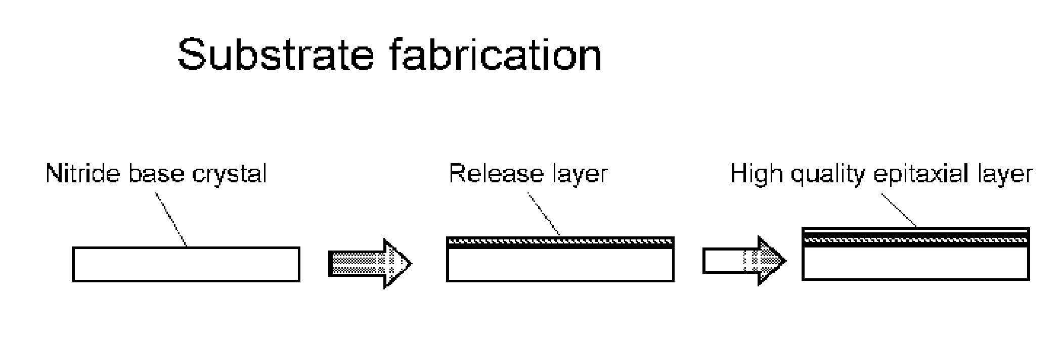
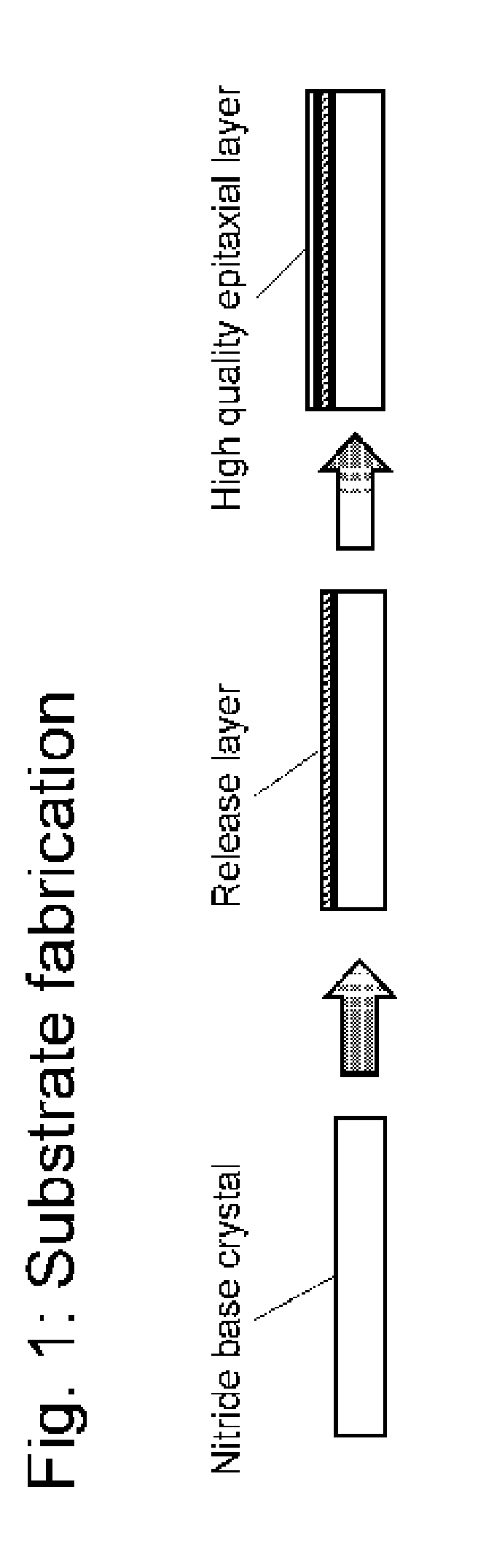
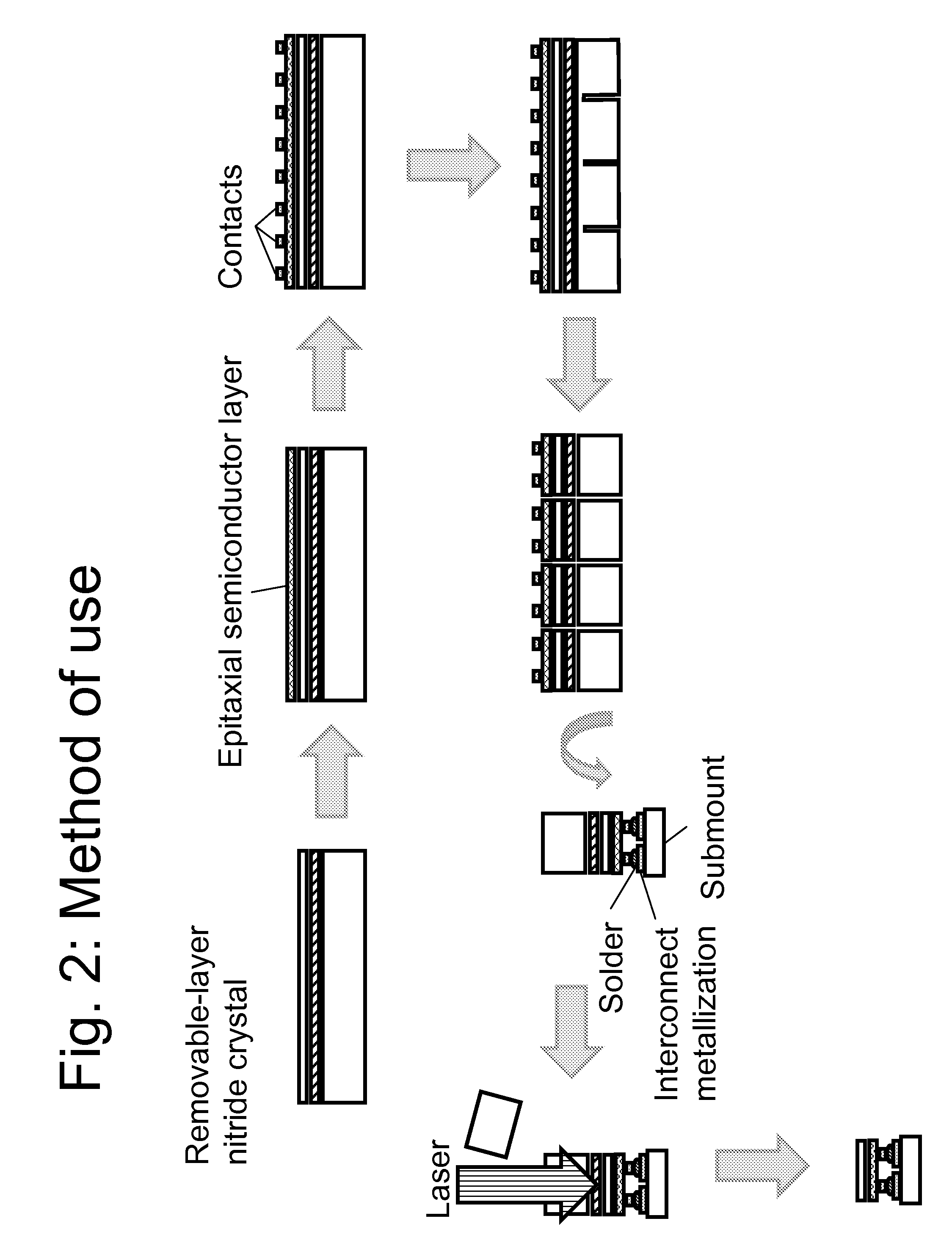
[0020]According to the present invention, techniques related to processing of crystals is provided. More particularly, the present invention provides a method for obtaining a gallium-containing nitride crystal with a release layer, but there can be others. In other embodiments, the present invention provides a method of manufacture of a high quality epitaxial gallium containing crystal with a release layer, but it would be recognized that other crystals and materials can also be processed. Such crystals and materials include, but are not limited to, GaN, AlN, InN, InGaN, AlGaN, and AlInGaN, and others for manufacture of bulk or patterned substrates. Such bulk or patterned substrates can be used for a variety of applications including optoelectronic devices, lasers, light emitting diodes, solar cells, photoelectrochemical water splitting and hydrogen generation, photodetectors, integrated circuits, and transistors, among other devices.

[0021]According to a specific embodiment, a start...


PUM

PropertyMeasurementUnit
optical absorption coefficientaaaaaaaaaa
thicknessaaaaaaaaaa

Abstract

A nitride crystal or wafer with a removable surface layer comprises a high quality nitride base crystal, a release layer, and a high quality epitaxial layer. The release layer has a large optical absorption coefficient at wavelengths where the base crystal is substantially transparent and may be etched under conditions where the nitride base crystal and the high quality epitaxial layer are not. The high quality epitaxial layer may be removed from the nitride base crystal by laser liftoff or by chemical etching after deposition of at least one epitaxial device layer. The nitride crystal with a removable surface layer is useful as a substrate for a light emitting diode, a laser diode, a transistor, a photodetector, a solar cell, or for photoelectrochemical water splitting for hydrogen generation.

Description

CROSS-REFERENCES TO RELATED APPLICATIONS[0001]This application claims priority to U.S. Provisional Patent Application No. 61 / 091,591, filed Aug. 25, 2008, commonly assigned, which is incorporated by reference in its entirety herein.STATEMENT AS TO RIGHTS TO INVENTIONS MADE UNDER FEDERALLY SPONSORED RESEARCH AND DEVELOPMENT[0002]Not ApplicableREFERENCE TO A “SEQUENCE LISTING,” A TABLE, OR A COMPUTER PROGRAM LISTING APPENDIX SUBMITTED ON A COMPACT DISK[0003]Not ApplicableBACKGROUND OF THE INVENTION[0004]The present invention generally relates to processing of crystals. More particularly, the present invention provides a method for obtaining a gallium-containing nitride crystal with a release layer, but there can be others. In other embodiments, the present invention provides a method of manufacture of a high quality epitaxial gallium containing crystal with a release layer, but it would be recognized that other crystals and materials can also be processed. Such crystals and materials ...

Claims


Application Information

Patent Timeline
Patent Type & Authority Patents(United States)
IPC IPC(8): H01L29/20
CPCC30B7/105C30B23/025C30B25/18C30B29/403C30B33/06H01L24/81H01L2224/0554H01L2224/05568H01L2224/05573H01L2224/056H01L2224/11H01L2224/81005H01L2224/81224H01L2924/00014H01L2924/14H01L2924/00H01L2224/05599H01L2224/0555H01L2224/0556
Inventor D'EVELYN, MARK P.
Owner SLT TECH
Why Eureka
Try Eureka