Method of fabricating an epitaxially grown layer on a composite structure

a composite structure and epitaxial growth technology, applied in the direction of basic electric elements, electrical apparatus, semiconductor devices, etc., can solve the problems of inability to use structures intended for detachment solutions described in those documents, growth structures that do not have the properties required for optimal use of devices, and stress applied at the bonding layer during high temperature epitaxial growth, and achieve the effect of not easy to creep

Active Publication Date: 2012-04-10
SOITEC SA
View PDF16 Cites 6 Cited by
  • Summary
  • Abstract
  • Description
  • Claims
  • Application Information

AI Technical Summary

Benefits of technology

[0011]Thus, by using a composite structure with a layer of oxide of silicon formed by LPCVD and with a thickness that is greater than or equal to that of the thin film, it is possible to control the phenomenon of the formation of microcavities buried in the bonding layer of oxide leading to delamination and to detachment of the support substrate in order, initially, to avoid deformation of the thin film and detachment of the support substrate over a limited period and then to activate the formation of microcavities in order to provoke detachment of the support substrate by rupture of the layer of oxide of silicon at the desired moment, i.e. before or after the end of epitaxy, or at the same time as the end of epitaxy.
[0012]As explained below in detail, using a bonding layer formed by LPCVD deposition with a thickness that is greater than that of the thin film prevents plastic (irreversible) deformations within the bonding layer. Thus, the formation of microcavities in the deposited bonding layer of oxide of silicon does not lead to delamination of the thin film nor does it buckle the surface of the film, even during heat treatments at a temperature that is higher than the oxide deposition temperature. Following a study, detailed below, concerning the temperature behavior of layers of oxide of silicon as a function of the deposition technique employed, the Applicant has determined that deposition by LPCVD can produce oxides with a temperature stability that is close to that of oxides obtained by thermal oxidation. Further, to withstand stresses due to the large difference between the low thermal expansion coefficient of the bonding layer of oxide of silicon and the high expansion coefficients of the materials of the composite structure, the thickness of the layer of oxide of silicon is greater than or equal to that of the thin film. This means that the stresses applied at the bonding layer during high temperature epitaxial growth can be reduced, as well as the risk of plastic deformations occurring in this bonding layer.
[0013]In order to detach the substrate at a predetermined moment (during or after epitaxial growth), it is necessary to apply a heat treatment at a temperature that is at least higher than the temperature at which the oxide of silicon is deposited, during a predetermined period that is a function of that temperature. The composite structure of the invention comprises a deposited bonding layer of oxide of silicon that is designed not to creep readily at the temperatures and stresses to which it is subjected during epitaxy. Since creep of the oxide results in the formation of microcavities, it is possible to initiate the formation of microcavities at a predetermined moment during epitaxy or thereafter by applying a heat treatment at a temperature that is above the oxide deposition temperature. This heat treatment can obtain creep of the bonding layer of oxide by increasing both the temperature of the oxide and that of the composite structure, causing the generation of stresses due to differences in the thermal expansion coefficients.
[0018]In a further aspect, the detachment method further comprises, after the heat treatment step, a complementary step of applying a mechanical separation stress at the bonding layer of oxide to provoke detachment of the support substrate. This complementary step may also consist of a chemical attack of the bonding layer of oxide to provoke detachment of the support substrate. Either way, because of the prior formation of microcavities, the heat treatment can weaken the bonding layer of oxide so that fracture / splitting is then readily obtained by mechanical or chemical action.
[0020]In accordance with one aspect of the invention, the method further comprises, prior to bonding, a step of densification heat treatment of the layer of oxide of silicon deposited by low pressure chemical vapor deposition on the bonding face of the support substrate and / or on the bonding face of the thin film. This densification heat treatment step can further increase the temperature behavior of the deposited oxide of silicon vis-à-vis the formation of microcavities. This step can, if necessary, reduce the ratio of the thicknesses of the thin film and of the deposited layer of oxide of silicon.

Problems solved by technology

However, such materials are not available in bulk form, in quantities, in diameters, or at prices that mean that they can be used on a large industrial scale.
Such growth structures do not have the properties required for optimal use in devices for use in optoelectronics, optics, or electronics.
The detachment solutions described in those documents cannot be used with structures that are intended to carry out epitaxial growth and that comprise materials with high thermal expansion coefficients such as sapphire, lithium tantalate, etc.
In fact, the bonding force obtained with the methods described in those documents is too low to be able, during heat treatments, to withstand the thermal expansion stresses induced by the materials used, or, during heteroepitaxy, to withstand the stresses induced by the crystalline lattice parameter differences.
With such materials, too low a bonding force means that a good quality structure for epitaxy cannot be formed, nor can the moment of detachment of the support substrate be controlled by applying an appropriate thermal budget.
In fact, when bonding is too weak, the support substrate risks becoming detached from the seed film at any time during the epitaxy process.

Method used


Image

  • Method of fabricating an epitaxially grown layer on a composite structure
  • Method of fabricating an epitaxially grown layer on a composite structure
  • Method of fabricating an epitaxially grown layer on a composite structure

Examples


Embodiment Construction

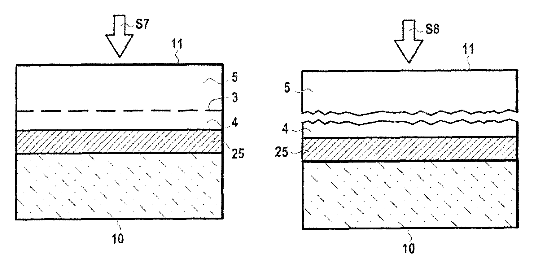
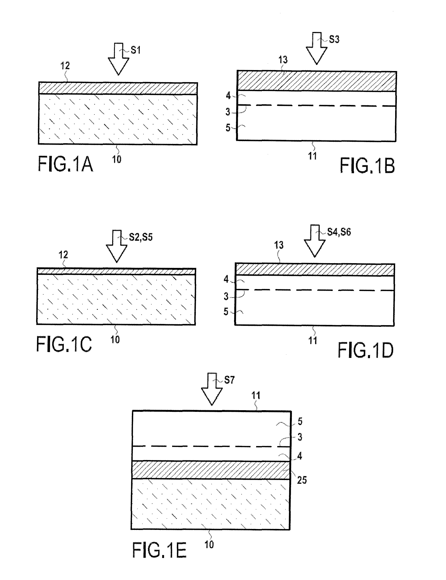
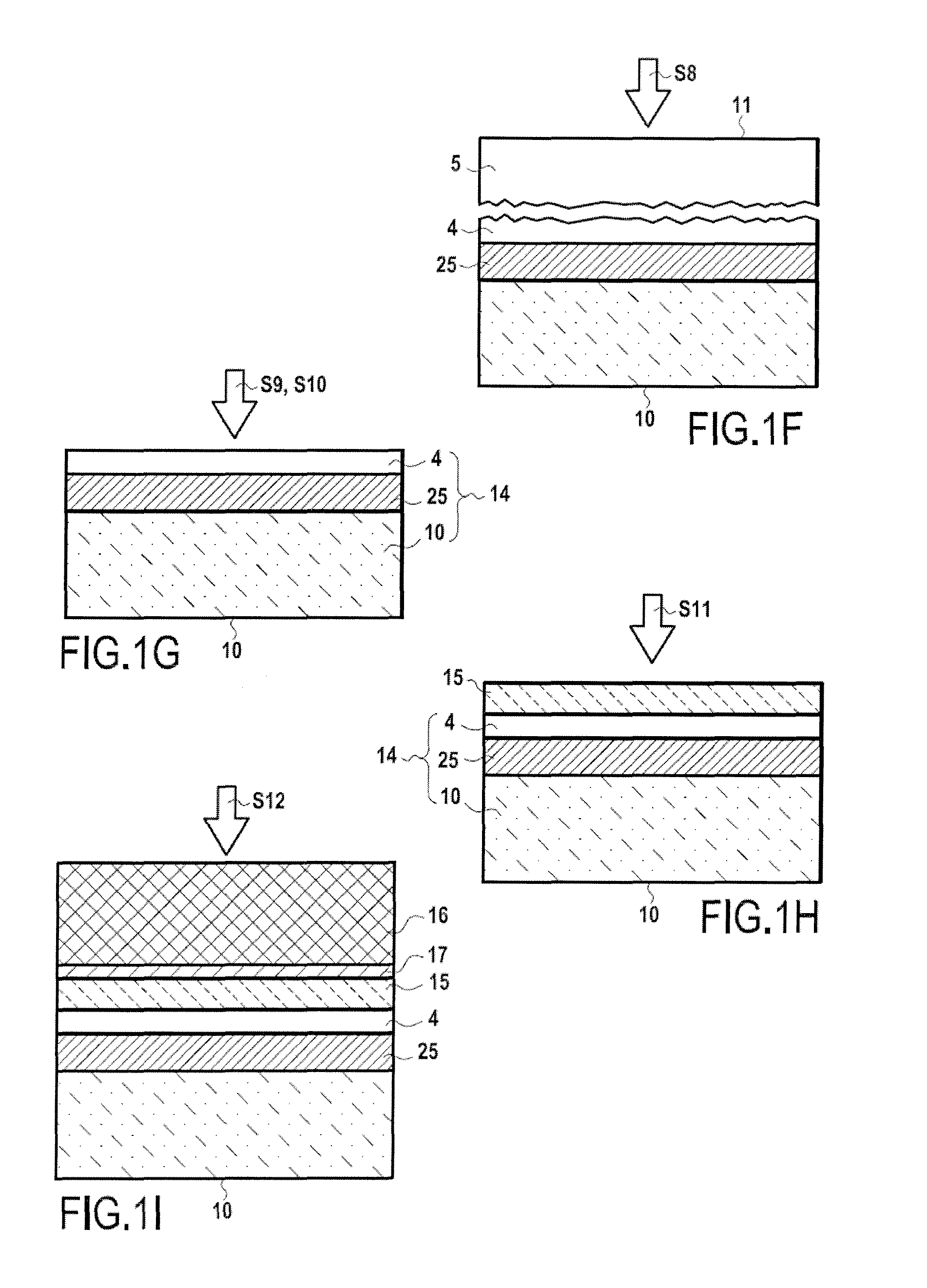
[0038]The present invention proposes the production of a composite structure allowing both the formation by epitaxy of layers of type III / N materials of good quality and detachment of the support substrate from the composition structure before or after the end of epitaxy, or substantially at the same time as the end of epitaxy.

[0039]To this end, the invention proposes a novel concept of a composite structure comprising a bonding layer of oxide located between the support substrate and the thin film and in which the formation of microcavities can be controlled. The composite structure of the invention means that microcavities in the bonding layer of oxide can be controlled both as regards preventing their appearance during heat treatments applied to the structure before and during at least a portion of the epitaxy and encouraging their formation or even their development during epitaxy or thereafter with a view to detachment of the support substrate.

[0040]The composite structure comp...


PUM

PropertyMeasurementUnit
temperatureaaaaaaaaaa
thicknessaaaaaaaaaa
thicknessaaaaaaaaaa

Abstract

A method of fabricating materials by epitaxy by epitaxially growing at least one layer of a material upon a composite structure that has at least one thin film bonded to a support substrate and a bonding layer of oxide formed by deposition between the support substrate and the thin film. The thin film and the support substrate have a mean thermal expansion coefficient of 7×10⁻⁶ K−1 or more. The bonding layer is formed by low pressure chemical vapor deposition (LPCVD) of a layer of silicon oxide on the bonding face of the support substrate or on the bonding face of the thin film. The thin film has a thickness of 5 micrometers or less while the thickness of the layer of oxide is equal to or greater than the thickness of the thin film. The method also includes a heat treatment carried out at a temperature that is higher than the temperature for deposition of the layer of oxide of silicon and for a predetermined period.

Description

[0001]This application is a 371 filing of International Patent Application PCT / EP2009 / 050086 filed Jan. 6, 2006.TECHNICAL FIELD AND PRIOR ART[0002]The present invention relates to the fabrication of layers grown epitaxially on a composite structure and to the detachment of such a layer from the structure. More precisely, the invention relates to the detachment of the support from the remainder of the composite structure after epitaxy, thereby enabling the support to be recycled, and the epitaxially grown layer to be released or to be transferred onto a final support if it is not self-supporting.[0003]Group III / N materials are endowed with particular electronic properties, such as a wide band-gap, which renders them highly advantageous for use in optics, optoelectronics, and electronics. However, such materials are not available in bulk form, in quantities, in diameters, or at prices that mean that they can be used on a large industrial scale. They are fabricated by heteroepitaxy on ...

Claims


Application Information

Patent Timeline
Patent Type & Authority Patents(United States)
IPC IPC(8): H01L21/76
CPCH01L21/76254H01L33/0079H01L2924/0002H01L2924/00H01L33/0093
Inventor FAURE, BRUCEMARCOVECCHIO, ALEXANDRA
Owner SOITEC SA
Why Eureka
Try Eureka