Interface, a method for observing an object within a non-vacuum environment and a scanning electron microscope

nvironment technology, applied in the field of interface, can solve the problems of reducing the throughput of scanning electron microscope and rendering such a scanning electron microscope impractical, and achieve the effect of improving detection

Active Publication Date: 2012-04-24
B NANO
View PDF15 Cites 32 Cited by
  • Summary
  • Abstract
  • Description
  • Claims
  • Application Information

AI Technical Summary

Benefits of technology

[0033]Conveniently, the method includes introducing a gas mixture into the non-vacuum environment such as to improve the detecting.
[0045]Conveniently, at least one aperture of the aperture array enables an acquisition of a higher resolution image than at least one other aperture of the aperture array.
[0051]Conveniently, at least one aperture of the aperture array enables an acquisition of a higher resolution image than at least one other aperture of the aperture array.
[0071]Conveniently, the scanning electron microscope is adapted to introduce a gas mixture into the non-vacuum environment such as to improve the detecting.

Problems solved by technology

Due to mechanical constraints, using an ultra thin membrane implies small supporting aperture.
The small size of the ultra thin membrane dramatically reduces the throughput of the scanning electron microscope and renders such a scanning electron microscope impractical.

Method used


Image

  • Interface, a method for observing an object within a non-vacuum environment and a scanning electron microscope
  • Interface, a method for observing an object within a non-vacuum environment and a scanning electron microscope
  • Interface, a method for observing an object within a non-vacuum environment and a scanning electron microscope

Examples


Embodiment Construction

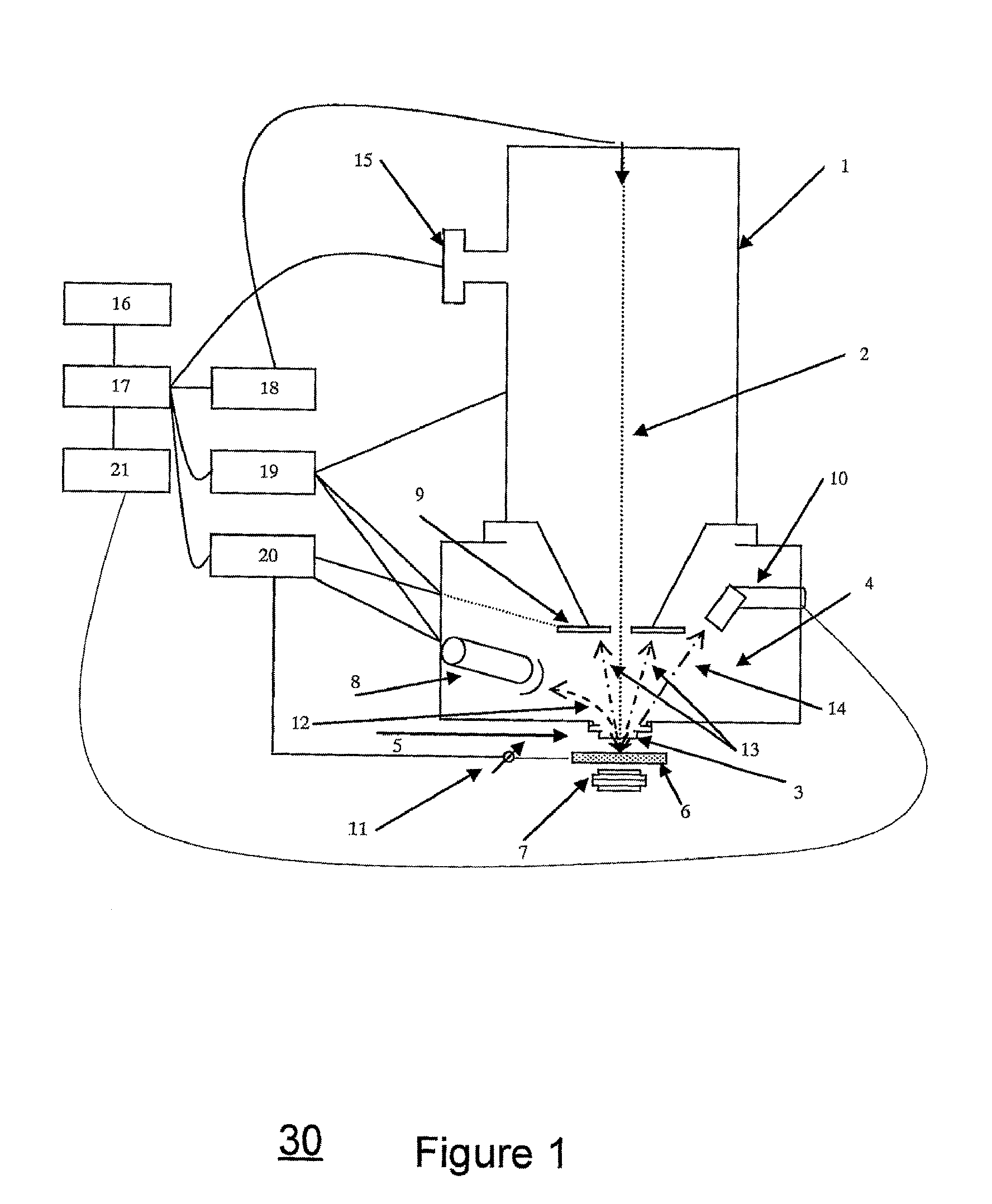
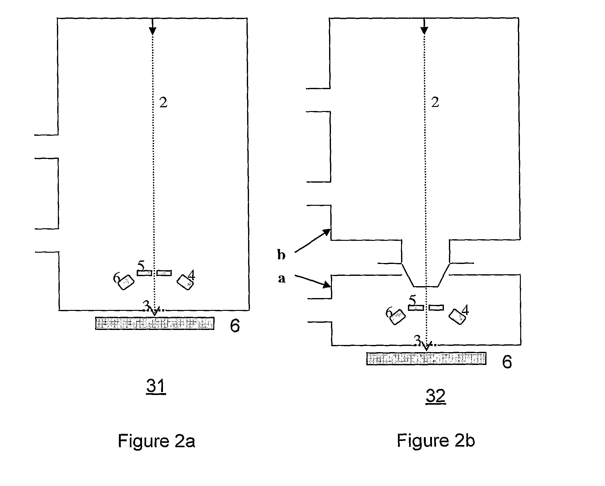
[0099]According to an embodiment of the invention the throughput of a scanning electron microscope that observes an object (positioned in a non-vacuum environment) is increased by illuminating multiple apertures (sealed by one or more membranes) simultaneously. These multiple apertures can form an aperture array or can be a part of an aperture array.

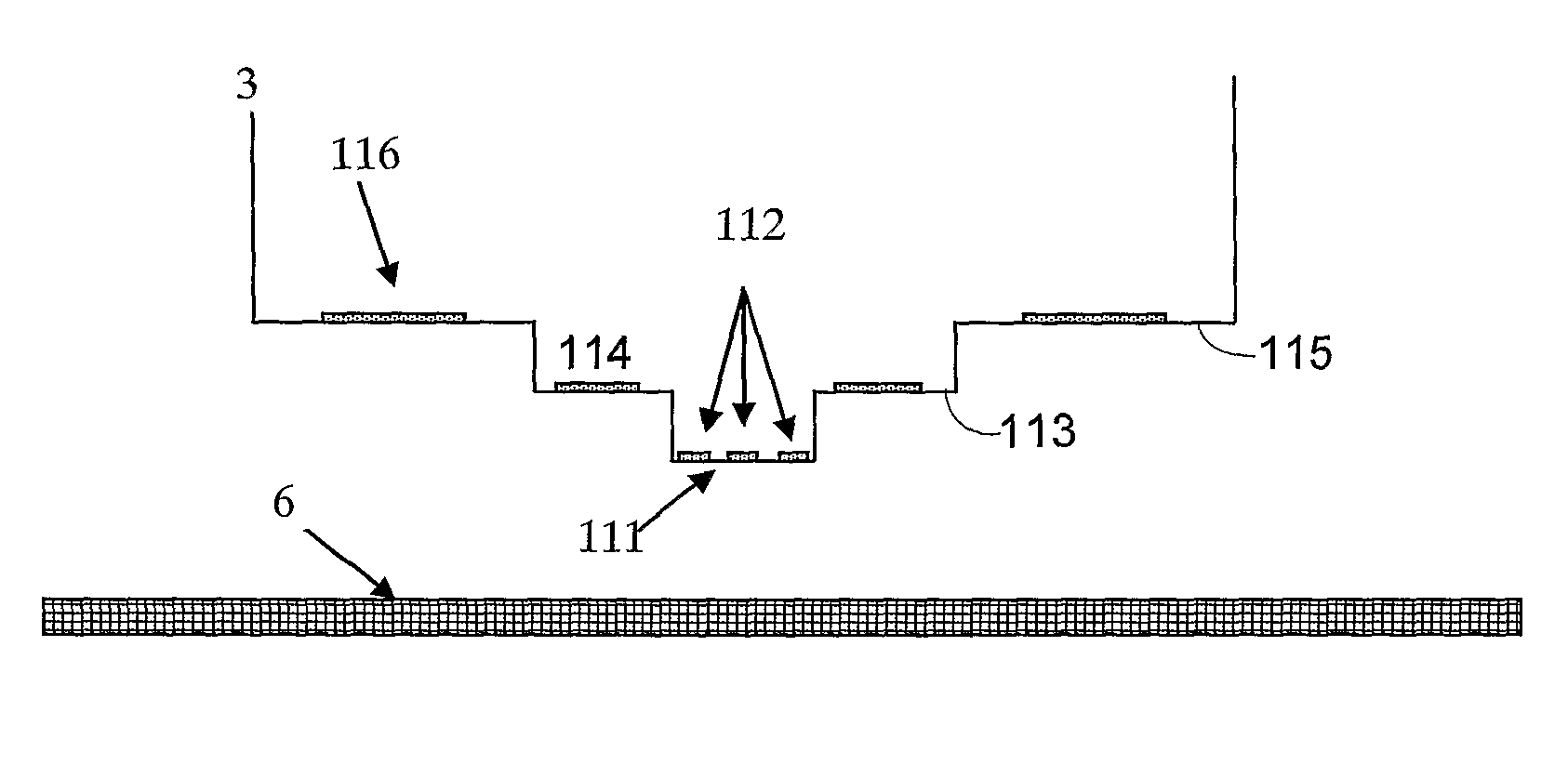
[0100]According to an embodiment of the invention one or more areas of an inspected object (positioned in a non-vacuum environment) are scanned by deflecting one or more electron beams and also introducing a corresponding mechanical movement of one or more apertures through which the one or more electron beams pass. This combination of deflection and mechanical movement increases the field of view of the system.

[0101]According to yet another embodiment of the invention multiple apertures that are sealed by one or more membranes are provided. The apertures and the membranes can differ by their size and thickness (of membranes) thus provid...


PUM

PropertyMeasurementUnit
thicknessaaaaaaaaaa
electron accelerating voltagesaaaaaaaaaa
thicknessaaaaaaaaaa

Abstract

An interface, a scanning electron microscope and a method for observing an object that is positioned in a non-vacuum environment. The method includes: passing at least one electron beam that is generated in a vacuum environment through at least one aperture out of an aperture array and through at least one ultra thin membrane that seals the at least one aperture; wherein the at least one electron beam is directed towards the object; wherein the at least one ultra thin membrane withstands a pressure difference between the vacuum environment and the non-vacuum environment; and detecting particles generated in response to an interaction between the at least one electron beam and the object.

Description

CROSS-REFERENCE TO RELATED APPLICATIONS[0001]This application is a National Phase Application of PCT International Application No. PCT / IL2007 / 001265, entitled “AN INTERFACE, A METHOD FOR OBSERVING AN OBJECT WITHIN A NON-VACUUM ENVIRONMENT AND A SCANNING ELECTRON MICROSCOPE”, International Filing Date Oct. 23, 2007, published on May 2, 2008 as International Publication No. WO 2008 / 050321, which in turn claims priority from U.S. Provisional Patent Ser. No. 60 / 862,631, filed Oct. 24, 2006, both of which are incorporated herein by reference in their entirety.BACKGROUND OF THE INVENTION[0002]High resolution microscopy is used in research and development, quality assurance and production in diverse fields such as material science, life science, the semiconductor industry and the food industry.[0003]Optical microscopy dating back to the seventeenth century, has reached its brick wall, defined by the wavelength of deep Ultra Violet photons, giving a finest resolution of about 80 nm. The pop...

Claims


Application Information

Patent Timeline
Patent Type & Authority Patents(United States)
IPC IPC(8): G01N23/00
CPCH01J37/20H01J37/28H01J37/301H01J37/06H01J37/285H01J2237/0458H01J2237/164H01J2237/2002H01J2237/2006H01J2237/2605H01J2237/28H01J2237/006H01J2237/15H01J2237/182H01J2237/2801H01J2237/2806H01J2237/2807
Inventor SHACHAL, DOV
Owner B NANO
Why Eureka
Try Eureka