Substrate for semiconductor device, semiconductor device, and electronic apparatus

a technology for semiconductor devices and substrates, applied in semiconductor devices, electrical devices, transistors, etc., can solve the problems of difficult to enhance the high-definition display capability of display devices such as electrophoretic display devices, and difficult to miniaturize transistors, so as to prevent leakage current generation or significantly reduce the effect of current generation

Active Publication Date: 2012-05-22
138 EAST LCD ADVANCEMENTS LTD
View PDF16 Cites 0 Cited by
  • Summary
  • Abstract
  • Description
  • Claims
  • Application Information

AI Technical Summary

Benefits of technology

[0007]An advantage of some aspects of the invention is to provide a substrate for a semiconductor device that makes it possible to prevent, or significantly reduce, the generation of a leakage current at a transistor without a drop in the ON current of the transistor, a semiconductor device that is provided with such a substrate, and an electronic apparatus that is provided with such a semiconductor device.
[0014]Because of the above relationship, it is possible to ensure that contact resistance between the floating electrode and the intermediate region is higher than each of contact resistance between the source electrode and the source region and contact resistance between the drain electrode and the drain region. Therefore, it is possible to ensure that, when a voltage is applied between the source electrode and the drain electrode, a voltage drop due to the contact resistance between the floating electrode and the intermediate region is larger than each of a voltage drop due to the contact resistance between the source electrode and the source region and a voltage drop due to the contact resistance between the drain electrode and the drain region. Thus, when the transistor is in its OFF state, it is possible to decrease the voltage applied to at least one of the plurality of channel regions (e.g., the channel region next to the drain region), and in addition thereto, to decrease the voltage applied between the gate electrode and the floating electrode (i.e., gate OFF bias). Consequently, it is possible to prevent the generation of a leakage current at the transistor when the transistor is in its OFF state. Moreover, when the transistor is in its ON state, a predetermined gate voltage (i.e., gate ON bias) is applied to the gate electrode. As a result, the contact resistance between the floating electrode and the intermediate region becomes lower than resistance at the channel region (i.e., channel resistance). Because of the lower contact resistance therebetween, there is almost no drop in an ON current, or there is no drop therein at all.
[0015]Furthermore, unlike the related-art structure disclosed in Japanese Patent No. 4275671, which includes two gate electrodes, the gate electrode according to the above aspect of the invention is formed as a single continuous electrode, for example, a single continuous rectangular electrode. Such a structure is advantageous in terms of easier patterning in manufacturing process, which makes it possible to miniaturize transistors.
[0016]As explained above, the substrate for a semiconductor device according to the first aspect of the invention makes it possible to prevent the generation of a leakage current at a transistor without a drop in the ON current of the transistor.

Problems solved by technology

However, the structure disclosed in Japanese Patent No. 4275671 has a technical problem in that, since each transistor has two gates, it will be difficult to miniaturize the transistor.
For this reason, it will be difficult to enhance the high-definition display capability of a display device such as an electrophoretic display device or the like.
The structure disclosed in Japanese Patent No. 4275671 has another technical problem as explained below.

Method used


Image

  • Substrate for semiconductor device, semiconductor device, and electronic apparatus
  • Substrate for semiconductor device, semiconductor device, and electronic apparatus
  • Substrate for semiconductor device, semiconductor device, and electronic apparatus

Examples


first embodiment

[0042]With reference to FIGS. 1 to 6, an electrophoretic display device according to a first embodiment of the invention is explained below.

[0043]First of all, an example of the general configuration of an electrophoretic display device according to the present embodiment of the invention is explained while referring to FIG. 1.

[0044]FIG. 1 is a block diagram that schematically illustrates an example of the general configuration of an electrophoretic display device according to an exemplary embodiment of the invention.

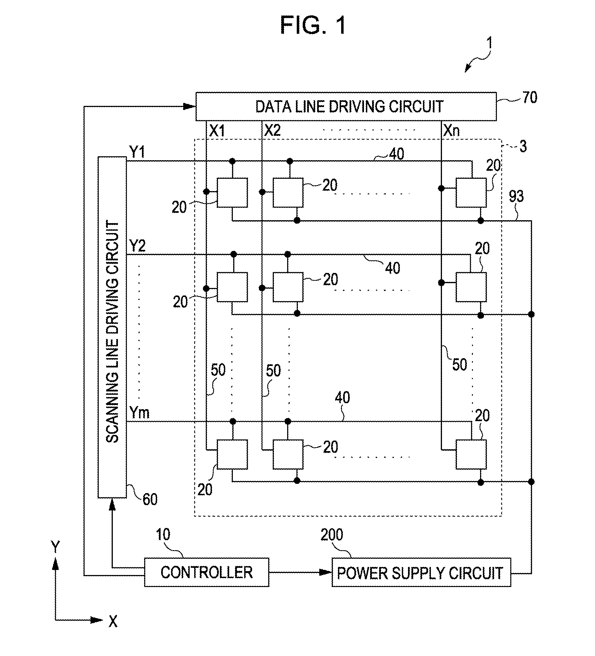
[0045]In FIG. 1, an electrophoretic display device 1 is provided with a display unit 3, a scanning line driving circuit 60, a data line driving circuit 70, a controller 10, and a power supply circuit 200.

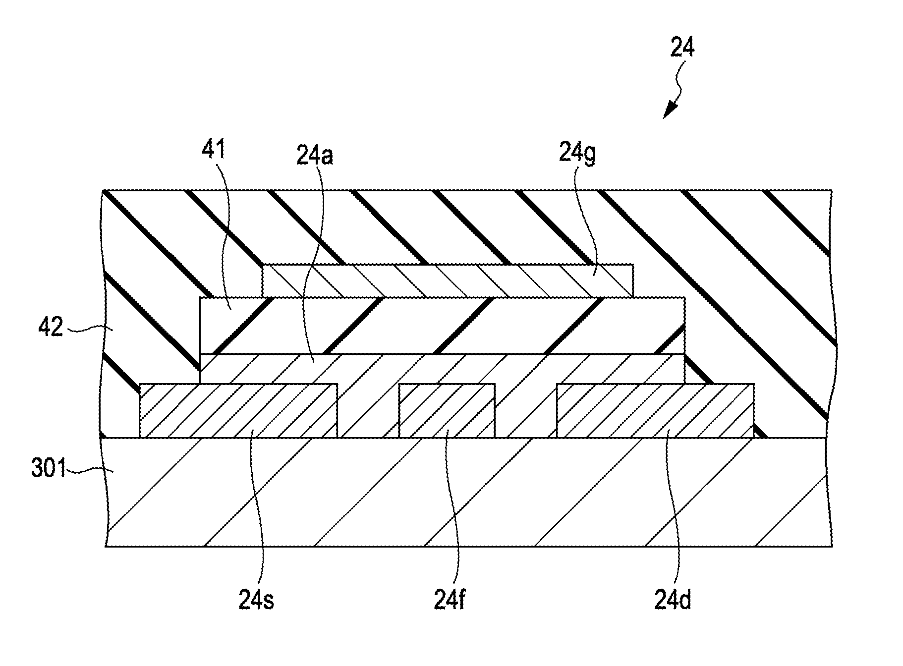
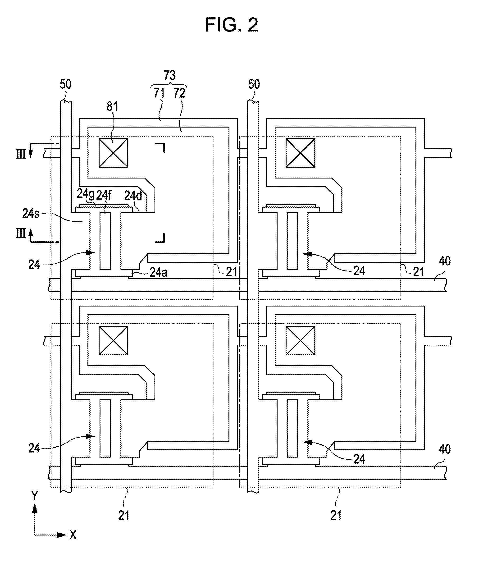
[0046]A plurality of pixels 20 is arranged in a matrix pattern in the display area 3. In a plan view, the pixel-array matrix is made up of “m” rows and “n” columns. In addition, m number of scanning lines 40, which are denoted as Y1, Y2, . . . , Ym in the accompanying d...


PUM


Abstract

A substrate for a semiconductor device includes: a base substrate; a semiconductor layer that has a source region, a drain region, a plurality of channel regions, and at least one intermediate region; a source electrode being in contact with the source region; a drain electrode being in contact with the drain region; a gate electrode that overlaps the plurality of channel regions, the intermediate region, and each of a part of the source electrode and a part of the drain electrode; and a floating electrode being in contact with the intermediate region. The size of an area where the floating electrode and the gate electrode overlap each other is smaller than the sum of the size of an area where the source electrode and the gate electrode overlap each other and the size of an area where the drain electrode and the gate electrode overlap each other.

Description

BACKGROUND[0001]1. Technical Field[0002]The present invention relates to a substrate for a semiconductor device, a semiconductor device that is provided with the substrate, and an electronic apparatus that is provided with the semiconductor device.[0003]2. Related Art[0004]A substrate that is used in a display device such as, for example, an electrophoretic display device that is driven in an active matrix scheme and includes a base substrate and a plurality of pixel-switching elements arranged over the base substrate is known as a type of a substrate for a semiconductor device. For example, a plurality of transistors each of which functions as the pixel-switching element is arranged over the base substrate. Such a substrate for a semiconductor device is sometimes called as an “active matrix substrate” or a “transistor array substrate”.[0005]As an example of related art, a transistor that functions as a pixel-switching element and has the following layered structure over the base su...

Claims


Application Information

Patent Timeline
Patent Type & Authority Patents(United States)
IPC IPC(8): H01L21/00
CPCH01L29/78696H01L29/78609
Inventor YAMAZAKI, YASUSHI
Owner 138 EAST LCD ADVANCEMENTS LTD
Why Eureka
Try Eureka