

Bi-directional multi-drop bus memory system
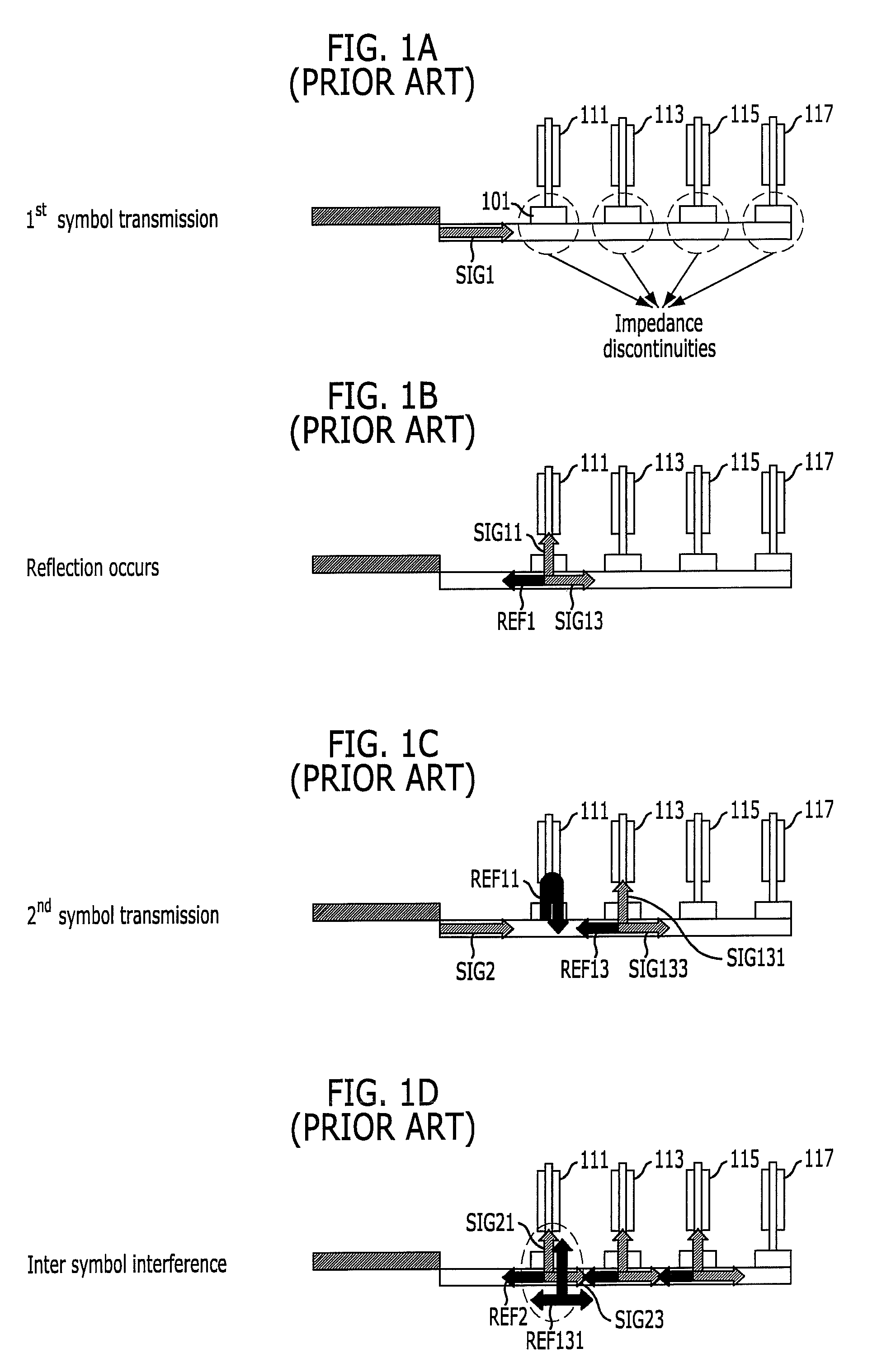
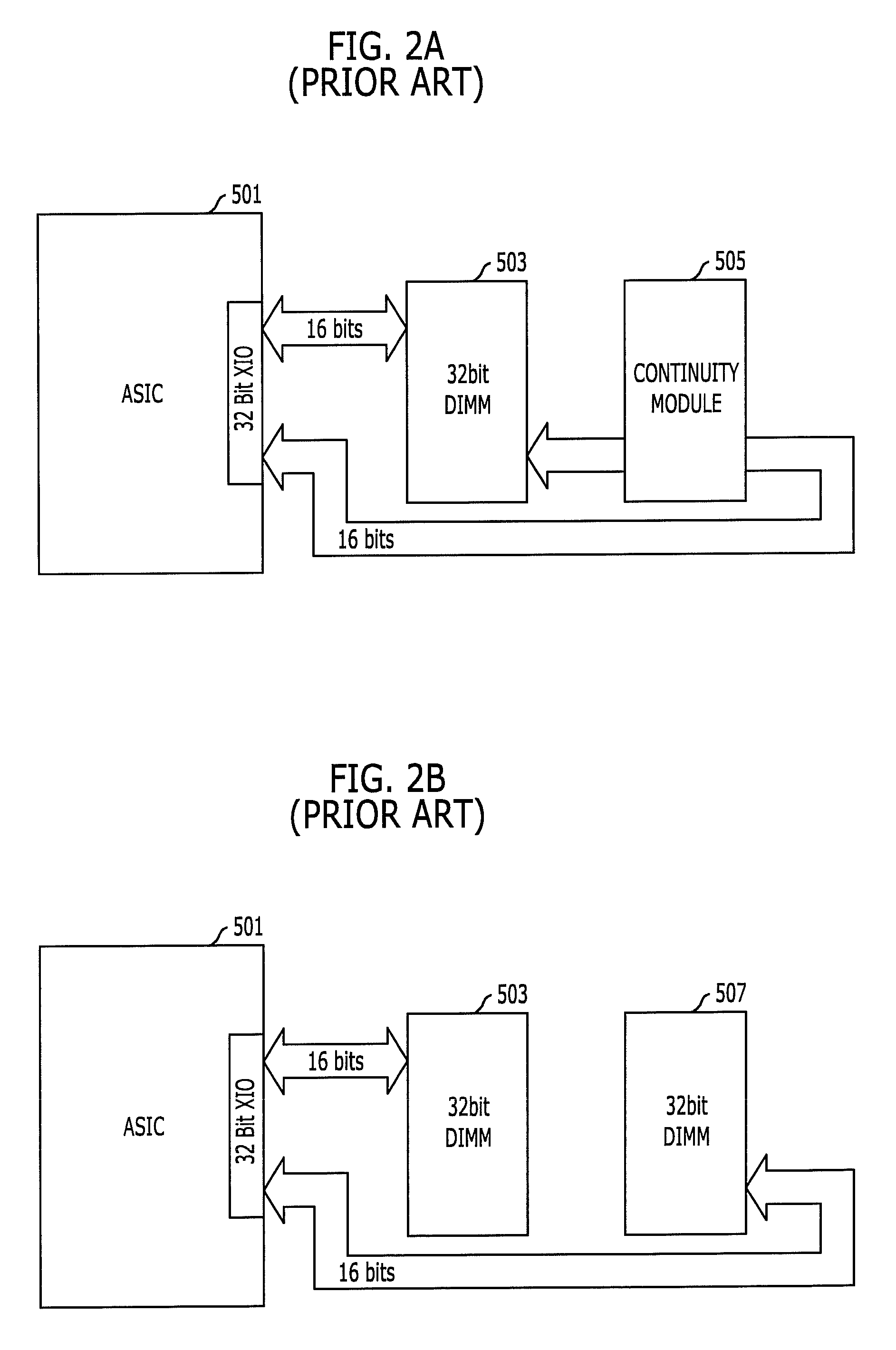
a bus memory and multi-drop technology, applied in the direction of logic circuit coupling/interface arrangement, pulse technique, instruments, etc., can solve the problems of greater than 2 gbps, inability to implement memory systems of large bandwidth, and sign integrity
- Summary
- Abstract
- Description
- Claims
- Application Information
AI Technical Summary
Benefits of technology
Problems solved by technology
Method used
Image

Examples
Embodiment Construction
[0044]Other objects and advantages of the present invention can be understood by the following description, and become apparent with reference to the embodiments of the present invention.
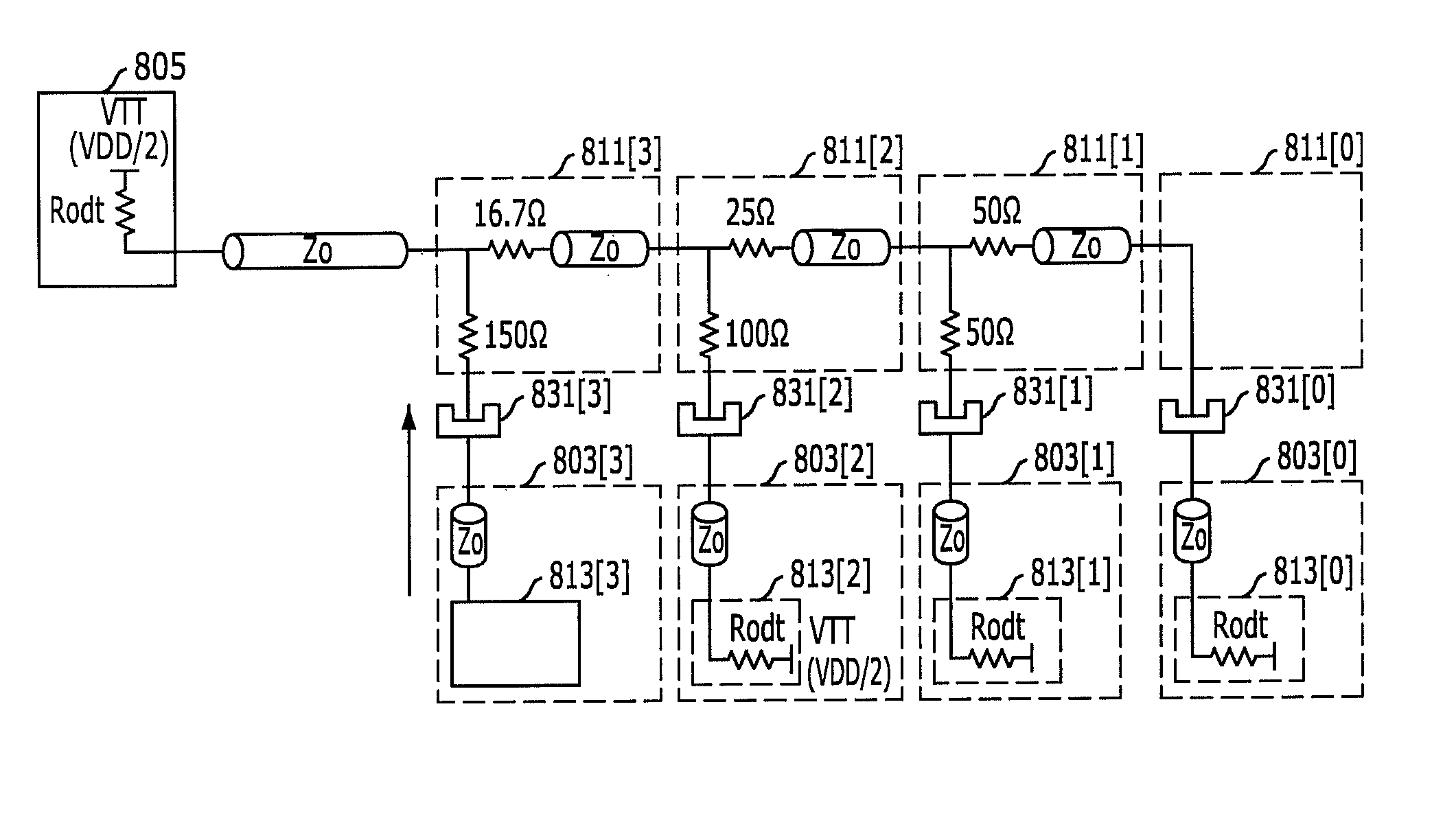
[0045]FIG. 4 is a schematic diagram describing an equivalent load of a transmission line.
[0046]The equivalent load ZTL1 loaded at a first terminal of a first transmission line TL1 is constituted with resistor loads AΩ and CΩ, which are physical elements, whose second terminals are coupled to the second terminal of the first transmission line TL1, and characteristic impedances DΩ and BΩ of second and third transmission lines TL2 and TL3 whose second terminals are coupled to first terminals of the resistor loads AΩ and CΩ. Because first terminals of the second and third transmission lines TL2 and TL3 are not seen at the first terminal of the first transmission line TL1, the equivalent load ZTL1 loaded at the first terminal of the first transmission line TL1 becomes (A+B)∥(C+D).
[0047]FIG. 5 is a schema...
PUM
 Abstract
Description
Claims
Application Information