Device and method of reducing junction leakage

a technology of junction leakage and device, applied in the direction of semiconductor devices, electrical equipment, transistors, etc., can solve the problems of reducing the thermal budget, incomplete removal of defects generated, and serious junction leakage, so as to reduce junction leakage and reduce junction leakage

Inactive Publication Date: 2012-06-19
GLOBALFOUNDRIES INC
View PDF5 Cites 8 Cited by
  • Summary
  • Abstract
  • Description
  • Claims
  • Application Information

AI Technical Summary

Benefits of technology

[0007]Another method for reducing junction leakage in a semiconductor device includes forming device isolation structures in a substrate; forming a gate stack having a first spacer formed on lateral sides thereof on the substrate; forming a faceted raised structure in a source / drain region of a device; diffusing dopants from the faceted raised structure into the substrate below the faceted raised structure to form source / drain regions; applying a sprinkle implantation on the faceted raised structure to produce a multi-depth dopant profile in the substrate for the source / drain regions; and forming a silicide on the faceted raised structures.
[0008]A semiconductor device includes a gate stack formed on a semiconductor substrate and source / drain regions formed adjacent to the gate stack having faceted raised structures formed on the substrate and having diffused dopant regions in the substrate below the faceted raised structures. A multi-depth dopant profile is formed in the substrate for the source / drain regions. The multi-depth dopant profile extends between the gate stack and a shallow trench isolation region and has a greatest depth at the shallow trench isolation region to reduce junction leakage.

Problems solved by technology

Junction leakage becomes a serious problem for low power technologies and particularly for technologies where devices are scaled beyond a 32 nm node.
This is done by reducing the thermal budget, which in turn results in incomplete removal of the defects generated by dopant ion implantation.
Also, with very shallow junctions, the space between a silicide and junction becomes small, which results in excessive junction leakage.
However, conventional raised source drain structure leads to excessive increases in the device parasitic capacitance.
Depending on the integration scheme, disposable spacers might be needed, which make the process more complicated.
In addition, there are concerns about junction leakage at an edge of the shallow trench isolation (STI).
Usually a divot exists at the STI edge and if the junction is not deep enough at this point, silicide formation at the STI edge causes additional leakage.

Method used


Image

  • Device and method of reducing junction leakage
  • Device and method of reducing junction leakage
  • Device and method of reducing junction leakage

Examples


Embodiment Construction

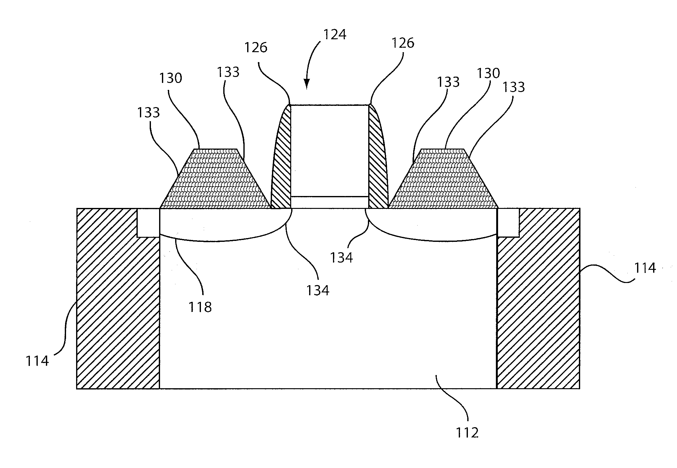
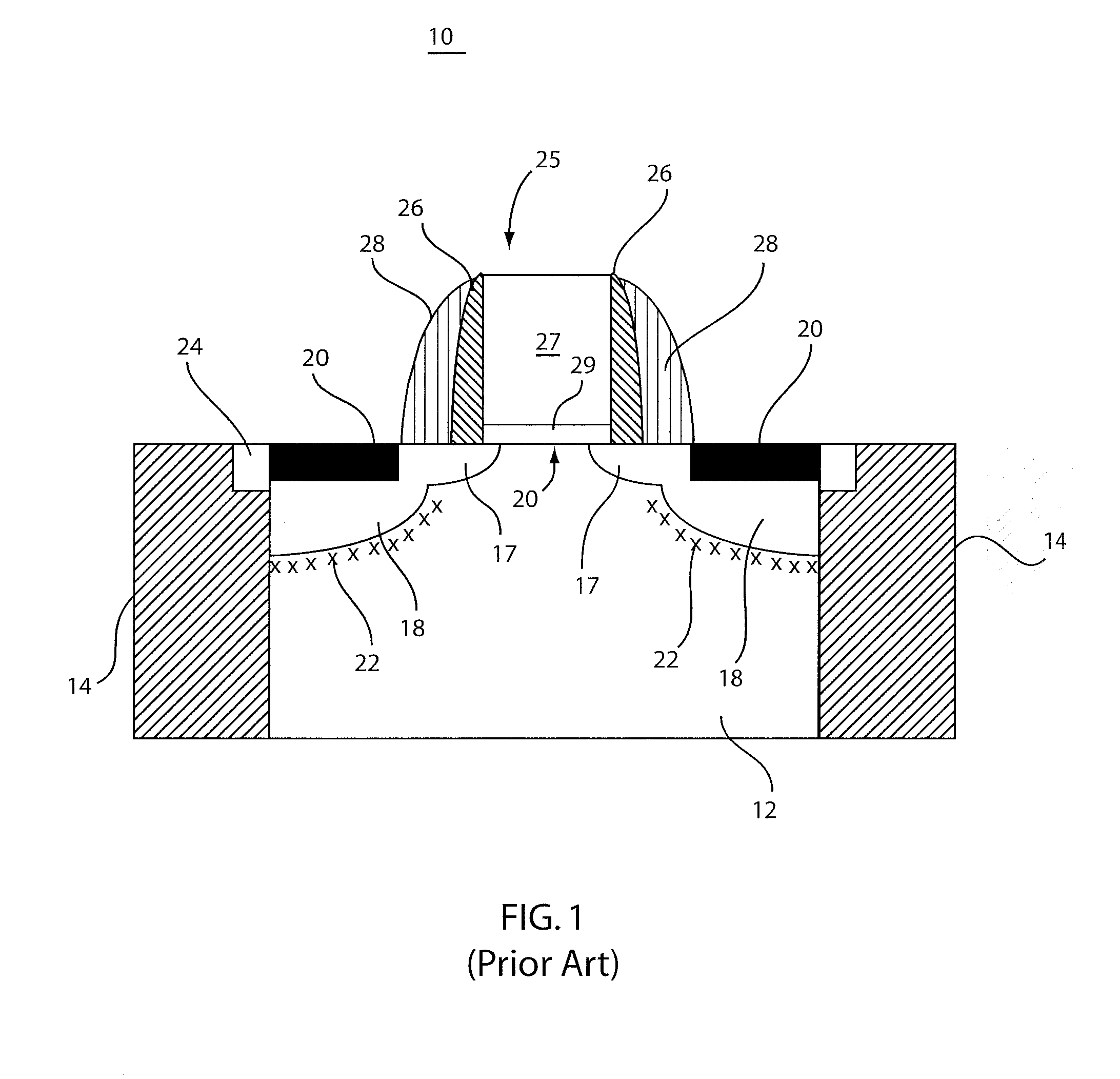
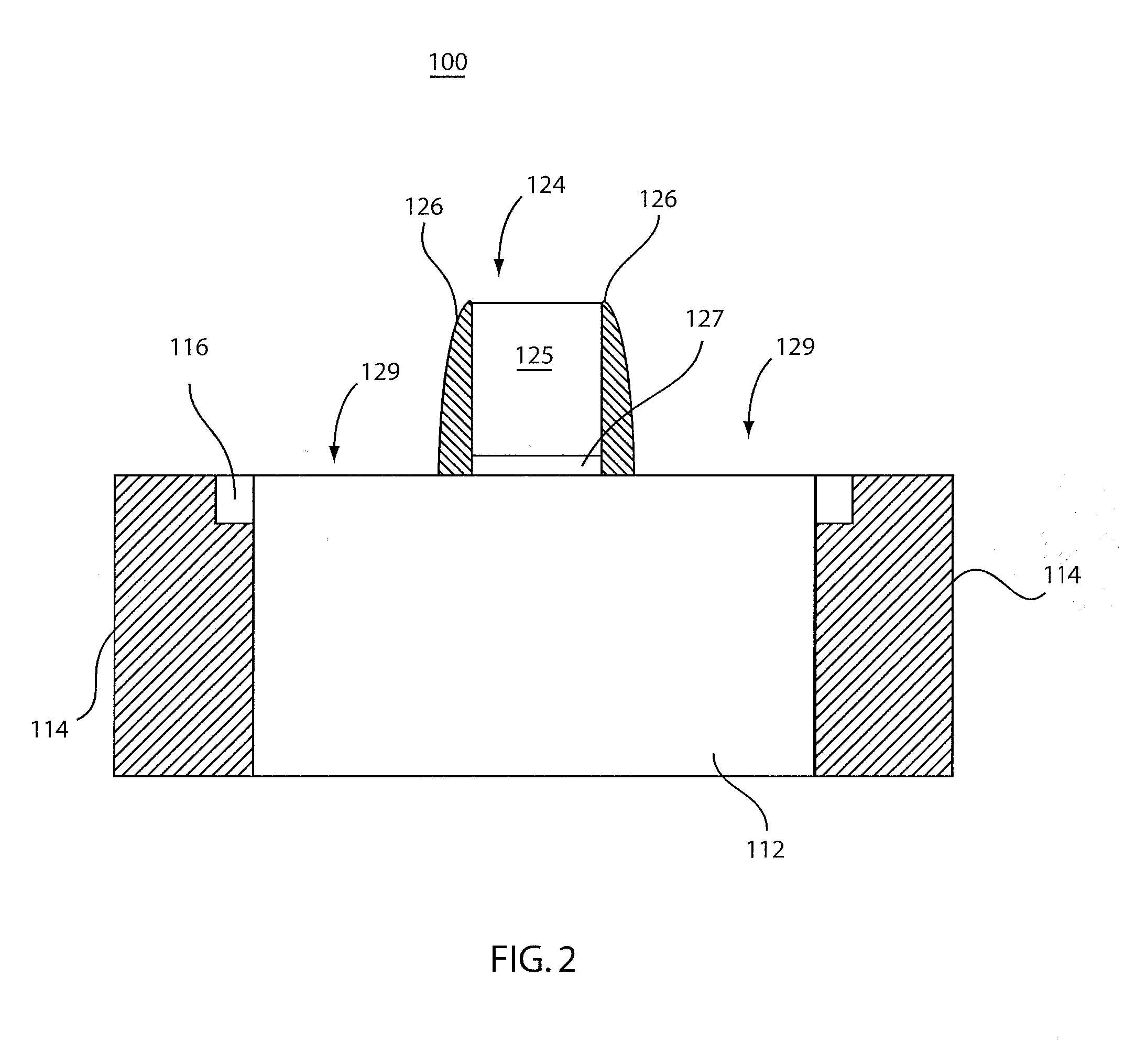
[0017]A faceted epitaxially raised source / drain structure and method are described to reduce the junction leakage in accordance with one embodiment. Source / drain (S / D) implantation is avoided to eliminate the generation of defects. A shallow junction is obtained which significantly reduces the junction capacitance and improves device short channel control. A low-dose “sprinkle” implant is used, which employs the facet nature of the epitaxial layer to reduce junction leakage at an edge of a shallow trench isolation (STI).

[0018]It is to be understood that the present invention will be described in terms of a given illustrative architecture; however, other architectures, structures, substrate materials and process features and steps may be varied within the scope of the present invention. The circuit as described herein may be part of a design for an integrated circuit chip. The chip design may be created in a graphical computer programming language, and stored in a computer storage me...


PUM


Abstract

A device and method for reducing junction leakage in a semiconductor junction includes forming a faceted raised structure in a source / drain region of the device. Dopants are diffused from the faceted raised structure into a substrate below the faceted raised structure to form source / drain regions. A sprinkle implantation is applied on the faceted raised structure to produce a multi-depth dopant profile in the substrate for the source / drain regions.

Description

BACKGROUND[0001]1. Technical Field[0002]The present invention relates to semiconductor devices and processing and more particularly to a structure and method for forming structures that reduce junction leakage.[0003]2. Description of the Related Art[0004]Junction leakage becomes a serious problem for low power technologies and particularly for technologies where devices are scaled beyond a 32 nm node. To control device short channel effects, dopant diffusion should be limited. This is done by reducing the thermal budget, which in turn results in incomplete removal of the defects generated by dopant ion implantation. Also, with very shallow junctions, the space between a silicide and junction becomes small, which results in excessive junction leakage.[0005]Raised source drain structures are considered as a way to alleviate these problems. However, conventional raised source drain structure leads to excessive increases in the device parasitic capacitance. Depending on the integration ...

Claims


Application Information

Patent Timeline
Patent Type & Authority Patents(United States)
IPC IPC(8): H01L21/335
CPCH01L21/26513H01L29/0847H01L29/665H01L29/6659H01L29/66628H01L29/7834H01L29/41783H01L29/6656H01L21/2658
Inventor CHENG, KANGGUODORIS, BRUCE B.KHAKIFIROOZ, ALIKULKARNI, PRANITASHAHIDI, GHAVAM G.
Owner GLOBALFOUNDRIES INC
Why Eureka
Try Eureka