Thin film transistor, display device using thin film transistor, and production method of thin film transistor

a technology of thin film transistor and production method, which is applied in the direction of transistors, semiconductor devices, electrical equipment, etc., can solve the problems of deterioration of electrical characteristics, malfunctions such as contrast deterioration, and the inability to obtain the threshold value which is necessary for operating a circuit, etc., and achieve the effect of increasing the number of production steps

Active Publication Date: 2012-06-26
CANON KK
View PDF16 Cites 40 Cited by
  • Summary
  • Abstract
  • Description
  • Claims
  • Application Information

AI Technical Summary

Problems solved by technology

As a common issue for the above-mentioned thin film transistors, there is deterioration of electrical characteristics when the semiconductor layer is exposed to light.
For example, in an active matrix liquid crystal display or an active matrix organic EL display, malfunctions such as deterioration in contrast occur because the OFF current in the transfer characteristics increases.
Further, occurrence of the shift in ON voltage makes conspicuous such malfunctions that a desired threshold value which is necessary for operating a circuit may not be obtained or an operating point of the circuit is shifted.
Therefore, if the ON voltage is shifted, a malfunction occurs in which desired emission intensity may not be obtained.
Therefore, steps of forming the light-shielding layers are necessary separately from the steps of forming the thin film transistor, which leads to an increase in the number of production steps.

Method used


Image

  • Thin film transistor, display device using thin film transistor, and production method of thin film transistor
  • Thin film transistor, display device using thin film transistor, and production method of thin film transistor
  • Thin film transistor, display device using thin film transistor, and production method of thin film transistor

Examples


first embodiment

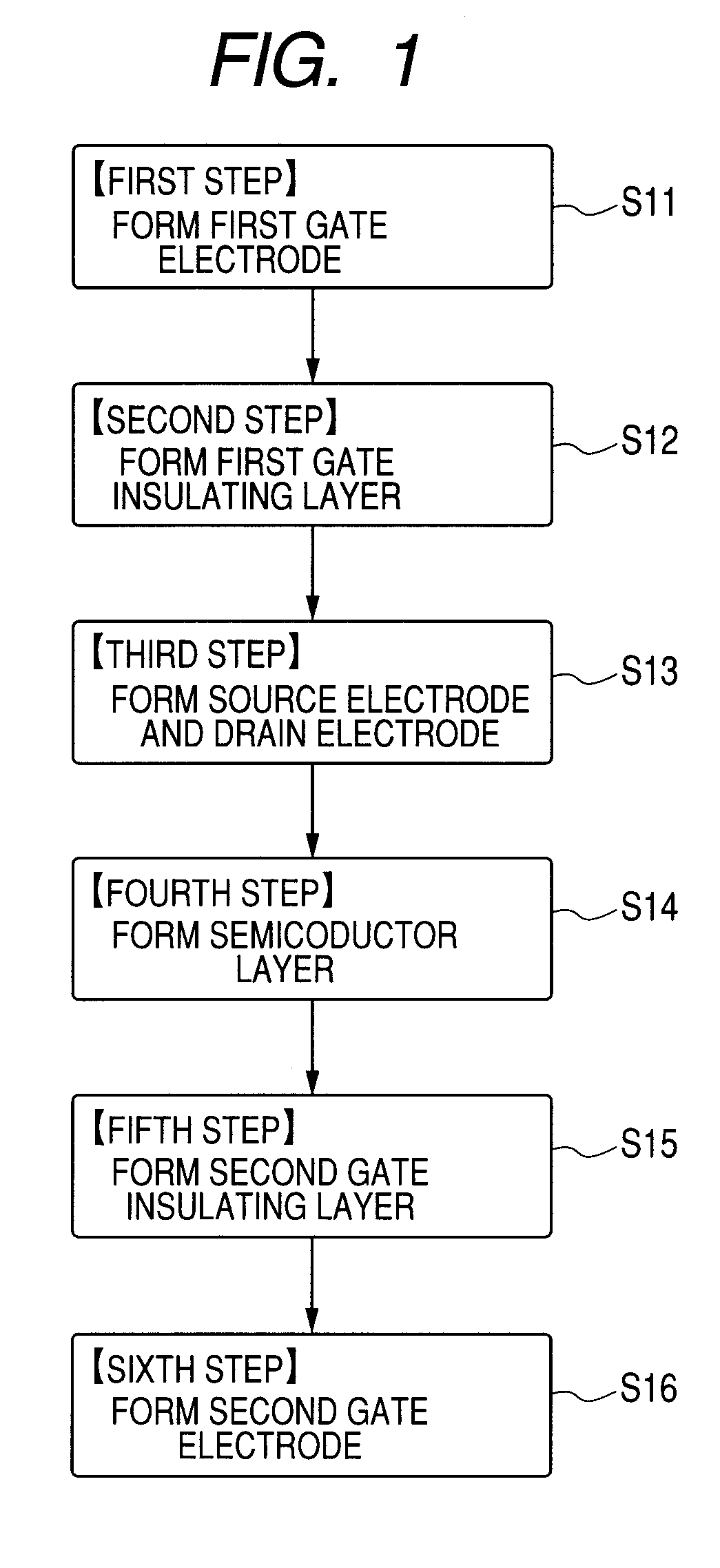
[0050](First Embodiment)

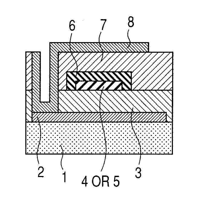
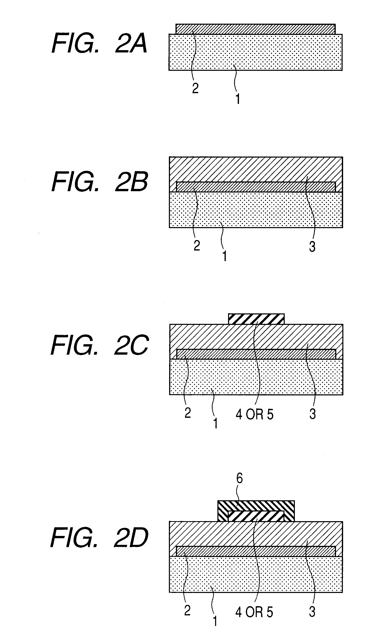
[0051]FIG. 3F is a cross-sectional view illustrating a structure of a thin film transistor according to a first embodiment of the present invention. As illustrated in FIG. 3F, this embodiment is an example of a bottom-contact type thin film transistor. The thin film transistor illustrated in FIGS. 3A to 3F is formed on the substrate 1. More specifically, the first gate electrode 2, the first gate insulating layer 3, the source electrode 4, the drain electrode 5, the semiconductor layer 6, the second gate insulating layer 7, and the second gate electrode 8 are formed on the substrate 1.

[0052]A glass substrate (Corning 1737) is used as the substrate 1. A thickness of the glass substrate is 0.5 mm. First, an Mo thin film with a thickness of 100 nm is formed on the substrate 1. In this embodiment, DC magnetron sputtering using an atmosphere of an argon gas is used to form the Mo thin film. Then, the deposited Mo thin film is processed by photolithography and dry ...

second embodiment

[0060](Second Embodiment)

[0061]FIG. 4H is a cross-sectional view illustrating a structure of a display device according to a second embodiment of the present invention. As illustrated in FIG. 4H, the display device according to this embodiment includes the thin film transistor described in the first embodiment and an organic EL element. A thin film transistor 100 illustrated in FIG. 4H is formed on the substrate 1. More specifically, the thin film transistor 100 includes the first gate electrode 2, the first gate insulating layer 3, the source electrode 4, the drain electrode 5, the semiconductor layer 6, the second gate insulating layer 7, and the second gate electrode 8. In addition, an organic EL element 200 illustrated in FIG. 4H is formed on the first gate insulating layer 3. More specifically, the organic EL element 200 includes a transparent anode electrode 9, a hole injecting layer 10, an organic light emitting layer 11, an electron injecting layer 12, and a cathode electrod...

third embodiment

[0073](Third Embodiment)

[0074]FIG. 8F is a cross-sectional view illustrating a structure of a thin film transistor according to a third embodiment of the present invention. In FIG. 8F, a cross-section perpendicular to a channel length direction of the thin film transistor (left) and a cross-section perpendicular to a channel width direction of the thin film transistor (right) are illustrated. As illustrated in FIG. 8F, this embodiment uses a channel-etch type thin film transistor as an example. Note that, in this embodiment, a case where the side-wall light-shielding layer is formed on both the sides of the semiconductor layer is described. However, by similar steps, the side-wall light-shielding layer may be formed only on one side of the semiconductor layer. The thin film transistor illustrated in FIGS. 8A to 8F is formed on the substrate 1. More specifically, the first gate electrode 2, the first gate insulating layer 3, the semiconductor layer 6, the source electrode 4, the drai...


PUM


Abstract

Provided is a thin film transistor including: a first gate electrode; a first gate insulating layer covering the first gate electrode; a semiconductor layer on the first gate insulating layer; a second gate insulating layer on the semiconductor layer; a second gate electrode on the second gate insulating layer; and a drain electrode and a source electrode electrically connected to the semiconductor layer, in which: the semiconductor layer is an amorphous oxide semiconductor containing at least one of Zn, Ga, In, and Sn; the first gate electrode shields light entering the semiconductor layer from below, and the second gate electrode shields light entering the semiconductor layer from above; and the second gate electrode is electrically connected to the first gate electrode by penetrating the first gate insulating layer and the second gate insulating layer, to thereby shield light entering the semiconductor layer from at least one of sides thereof.

Description

BACKGROUND OF THE INVENTION[0001]1. Field of the Invention[0002]The present invention relates to a thin film transistor, a display device using the thin film transistor, and a production method of the thin film transistor. More particularly, the present invention relates to a double-gate thin film transistor, a display device using the double-gate thin film transistor, and a production method for the double-gate thin film transistor. Note that, in this specification, the term “double-gate” refers to a structure in which gate electrodes are disposed on an upper side (one surface side) and a lower side (another surface side) of a semiconductor layer through an intermediation of gate insulating films.[0003]2. Description of the Related Art[0004]A thin film transistor is a kind of a field-effect transistor and is mainly applied to an active matrix liquid crystal display or an active matrix organic electroluminescence (EL) display. At present, the mainstream is a polycrystalline silicon ...

Claims


Application Information

Patent Timeline
Patent Type & Authority Patents(United States)
IPC IPC(8): H01L29/22
CPCH01L29/7869H01L27/1225
Inventor TAKAHASHI, KENJIHAYASHI, RYOYAGINUMA, SEIICHIRO
Owner CANON KK
Why Eureka
Try Eureka