Array substrate and manufacturing method thereof, and display device

A technology of an array substrate and a manufacturing method, which is applied in the fields of an array substrate and its manufacturing method and a display device, can solve problems affecting the characteristics of oxide-TFT transistors, etc., and achieve the effect of preventing adverse effects

Active Publication Date: 2017-10-20
BOE TECH GRP CO LTD
View PDF3 Cites 31 Cited by
  • Summary
  • Abstract
  • Description
  • Claims
  • Application Information

AI Technical Summary

Problems solved by technology

[0004] Based on the above, the development of the LTPO process has high value and significance, but in the existing LTPO process, an Oxide layer needs to be formed on the LTPS layer, and the Oxide process involves multi-step heat treatment and annealing processes, which will lead to LTPS- The hydrog

Method used


Image

  • Array substrate and manufacturing method thereof, and display device
  • Array substrate and manufacturing method thereof, and display device
  • Array substrate and manufacturing method thereof, and display device

Examples


Embodiment Construction

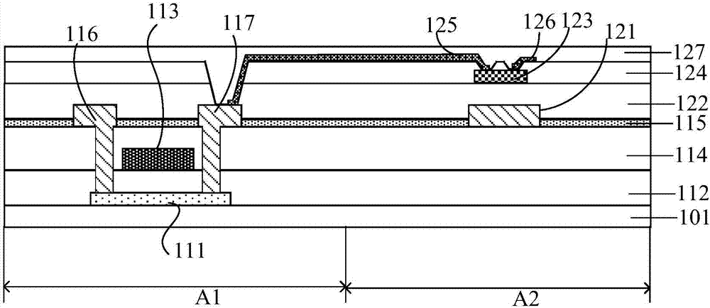
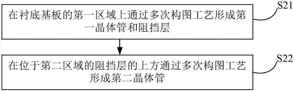
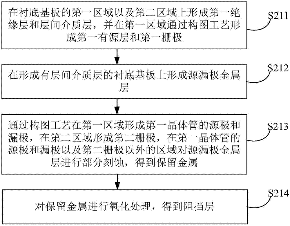
[0042] Example embodiments will now be described more fully with reference to the accompanying drawings. Example embodiments may, however, be embodied in many forms and should not be construed as limited to the examples set forth herein; rather, these embodiments are provided so that this disclosure will be thorough and complete and will fully convey the concept of example embodiments to those skilled in the art. The drawings are merely schematic illustrations of the present disclosure and are not necessarily drawn to scale. The same reference numerals in the drawings denote the same or similar parts, and thus their repeated descriptions will be omitted.

[0043] Furthermore, the described features, structures, or characteristics may be combined in any suitable manner in one or more embodiments. In the following description, numerous specific details are provided in order to give a thorough understanding of embodiments of the present disclosure. However, those skilled in th...


PUM


Abstract

The invention discloses an array substrate and a manufacturing method thereof, and a display device. The array substrate comprises a substrate, wherein a first region and a second region of the substrate are respectively provided with a first transistor and a second transistor, the first transistor has a first active layer, the first active layer is low temperature polysilicon, the second transistor has a second active layer, the second active layer is metal-oxide semiconductor, the first active layer, an interlayer dielectric layer and the second active layer are sequentially arranged on the substrate, and a blocking layer is arranged between the interlayer dielectric layer and the second active layer. The array substrate is advantaged in that through arranging the blocking layer, the insulation and hydrogen blocking effect between the interlayer dielectric layer of the low temperature polysilicon film transistor and the active layer of the oxide film transistor is realized, hydrogen penetration in the subsequent heat treatment technology between the low temperature polysilicon film transistor and the oxide film transistor can be prevented, and bad influence of transistor characteristics of the low temperature polycrystalline silicon film transistor and the oxide film transistor can be prevented.

Description

technical field [0001] The present disclosure relates to the field of display technology, in particular, to an array substrate, a manufacturing method thereof, and a display device. Background technique [0002] At present, AMOLED (Active Matrix Organic Light Emitting Diode, active matrix organic light emitting diode) technology is the development trend of electronic products, because of its wider viewing angle, higher refresh rate and thinner size, it is widely used in smartphones. been widely applied. [0003] LTPO (Low Temperature Polycrystalline Oxide, Low Temperature Polycrystalline Oxide) technology combines LTPS-TFT (Low Temperature Poly-silicon Thin Film Transistor, Low Temperature Polycrystalline Silicon Thin Film Transistor) and Oxide-TFT (Oxide Thin Film Transistor). The advantage of AMOLED products has certain technical advantages in high PPI (Pixels Per Inch, pixel density), low power consumption, high image quality, etc. In addition, due to the advantages of l...

Claims


Application Information

Patent Timeline
IPC IPC(8): H01L27/12H01L29/06H01L29/786H01L21/77
CPCH01L27/1222H01L27/1225H01L27/1259H01L29/0649H01L29/78606H01L27/1248H01L27/1251H01L27/127
Inventor 李海旭曹占锋姚琪
Owner BOE TECH GRP CO LTD
Why Eureka
Try Eureka