Array substrate, manufacturing method thereof and display device

A technology of an array substrate and a manufacturing method, applied in the display field, can solve the problem that polysilicon thin film transistors cannot be applied to the production of large-size display panels and the like

Inactive Publication Date: 2015-04-22
BOE TECH GRP CO LTD
View PDF3 Cites 31 Cited by
  • Summary
  • Abstract
  • Description
  • Claims
  • Application Information

AI Technical Summary

Problems solved by technology

[0005] The invention provides an array substrate, a manufacturing method thereof, and a display device, which can effectively so

Method used


Image

  • Array substrate, manufacturing method thereof and display device
  • Array substrate, manufacturing method thereof and display device
  • Array substrate, manufacturing method thereof and display device

Examples


Embodiment 1

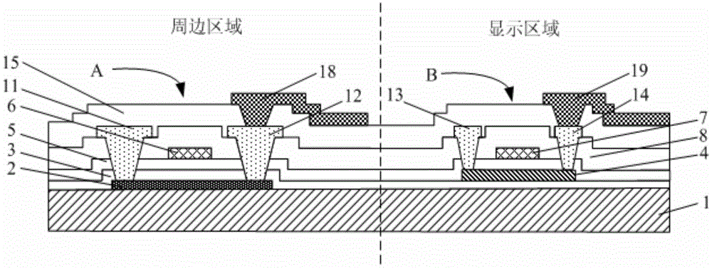
[0094] figure 1 A schematic cross-sectional view of the array substrate provided in Embodiment 1 of the present invention, as shown in figure 1 As shown, the array substrate includes: a first thin film transistor A and a second thin film transistor B, the first thin film transistor A and the second thin film transistor B are formed above the base substrate 1, the first thin film transistor A is a polysilicon thin film transistor, The second thin film transistor B is a metal oxide thin film transistor, the first thin film transistor A is located in the peripheral area of ​​the array substrate, and the second thin film transistor is located in the display area B of the array substrate.

[0095] In this embodiment, on the one hand, a polysilicon thin film transistor with relatively high electron mobility (electron mobility at 30 cm 2 / Vs or so) is arranged in the peripheral area of ​​the array substrate, which can meet the high requirements of the peripheral area of ​​the large-...

Embodiment 2

[0133] Figure 4 A schematic cross-sectional view of the array substrate provided in Embodiment 1 of the present invention, as shown in Figure 4 As shown, the array substrate includes: a first thin film transistor C and a second thin film transistor D, the first thin film transistor C and the second thin film transistor D are formed above the base substrate 1, the first thin film transistor C is a polysilicon thin film transistor, The second thin film transistor D is an amorphous silicon thin film transistor, the first thin film transistor C is located in the peripheral area of ​​the array substrate, and the second thin film transistor D is located in the display area of ​​the array substrate.

[0134] In this embodiment, on the one hand, polysilicon thin film transistors with relatively high electron mobility are arranged in the peripheral area of ​​the array substrate, which can meet the high requirement of the electronic mobility of the components in the peripheral area of...

Embodiment 3

[0163] Embodiment 3 of the present invention provides a display device. The display device includes an array substrate. The array substrate adopts the array substrate provided in Embodiment 1 or Embodiment 2 above. For details, please refer to the above-mentioned Embodiment 1 and Embodiment 2. description and will not be repeated here.

[0164] The display device in this embodiment can be any product or component with a display function, such as a liquid crystal panel, an electronic paper, an OLED panel, a mobile phone, a tablet computer, a television set, a monitor, a notebook computer, a digital photo frame, or a navigator.

[0165] Since the display device provided in the third embodiment includes the array substrate in the first or second embodiment above, this embodiment has the beneficial technical effects described in the first or second embodiment above.


PUM


Abstract

The invention discloses an array substrate, a manufacturing method of the array substrate and a display device. The array substrate comprises a first thin film transistor and a second thin film transistor. The first thin film transistor and the second thin film transistor are formed above an underlayer substrate. The first thin film transistor is a polycrystalline silicon thin film transistor. The second thin film transistor is a metallic oxide thin film transistor or an amorphous silicon thin film transistor. The first thin film transistor is located on the peripheral region of the array substrate, and the second thin film transistor is located on the display region of the array substrate. By means of the technical scheme, the problem that the polycrystalline silicon thin film transistor cannot be applied to production of large display panels with the ram being over 6 G is solved, the limit of the excimer laser crystallization process bottleneck is broken through thoroughly, and the array substrate, the manufacturing method and the display device have very high application value.

Description

technical field [0001] The present invention relates to the field of display technology, in particular to an array substrate, a manufacturing method thereof, and a display device. Background technique [0002] As the size of the display panel continues to increase and the frequency of the driving circuit increases, the integration level of the peripheral area of ​​the display panel will also increase accordingly. The electron mobility of the existing amorphous silicon thin film transistors is difficult to meet the working requirements. For this reason, manufacturers replace the amorphous silicon thin film transistors in the display panel with polysilicon thin film transistors with higher electron mobility. [0003] In the prior art, when preparing a polysilicon layer, the following three technologies are often used for preparation: solid phase crystallization (Solid Phase Crystallization, referred to as SPC), metal-induced lateral crystallization (Metal-Induced Lateral Cryst...

Claims


Application Information

Patent Timeline
IPC IPC(8): H01L21/77H01L27/12
CPCH01L21/77H01L27/1214H01L27/1259H01L27/1225
Inventor 刘翔
Owner BOE TECH GRP CO LTD
Why Eureka
Try Eureka