Thin film transistor and manufacturing method thereof, array substrate and display device

A technology for thin film transistors and a manufacturing method, applied in the field of liquid crystal display, can solve the problems of poor film stability and reduced film deposition rate, and achieve the effects of reducing hydrogen content, fully decomposing silane, and avoiding metal oxide reactions

Active Publication Date: 2014-06-25
BEIJING BOE OPTOELECTRONCIS TECH CO LTD
View PDF5 Cites 32 Cited by
  • Summary
  • Abstract
  • Description
  • Claims
  • Application Information

AI Technical Summary

Problems solved by technology

The purpose of the etching barrier layer process is to avoid the corrosion of the metal by the etchant during the etching process of the source and drain electrodes on the one hand; on the other hand, the etching barrier layer process usually uses silicon oxide materials to ensure that the silicon oxide film To maintain a low hydrogen content, the plasma-enhanced chemical vapor deposition method (PECVD) is usually used to deposit silicon oxide films. For example,

Method used


Image

  • Thin film transistor and manufacturing method thereof, array substrate and display device
  • Thin film transistor and manufacturing method thereof, array substrate and display device
  • Thin film transistor and manufacturing method thereof, array substrate and display device

Examples


Embodiment Construction
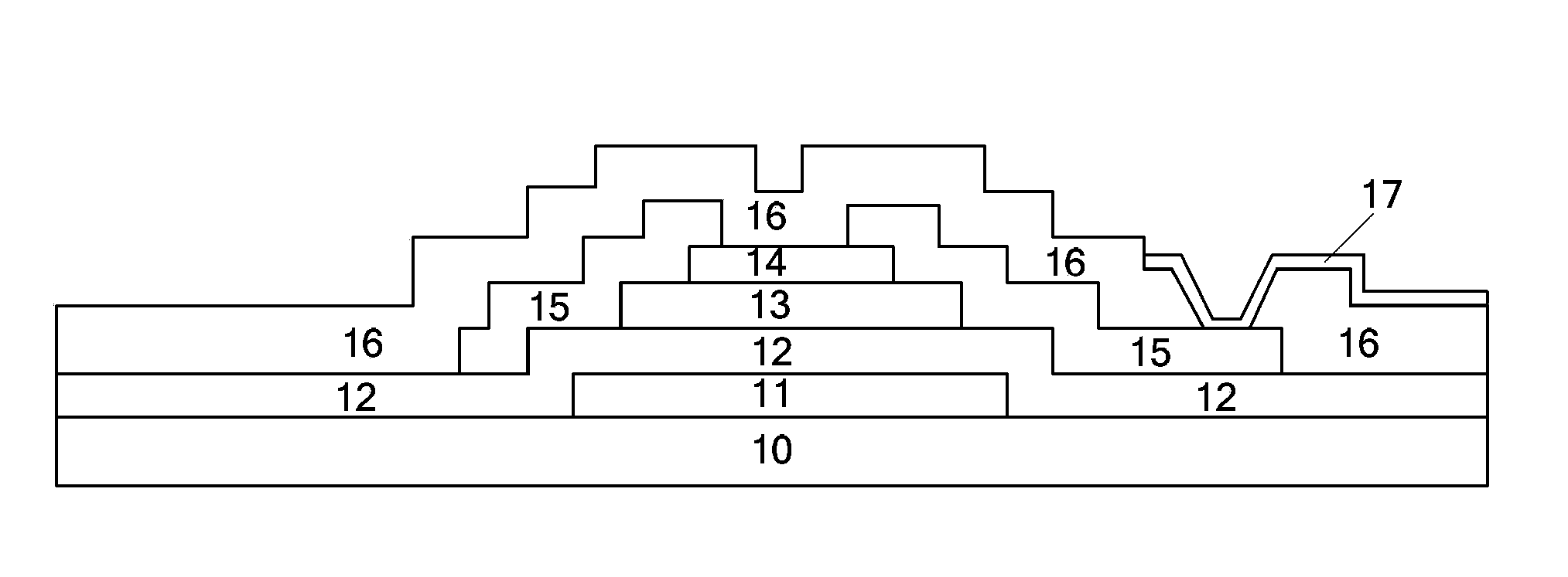
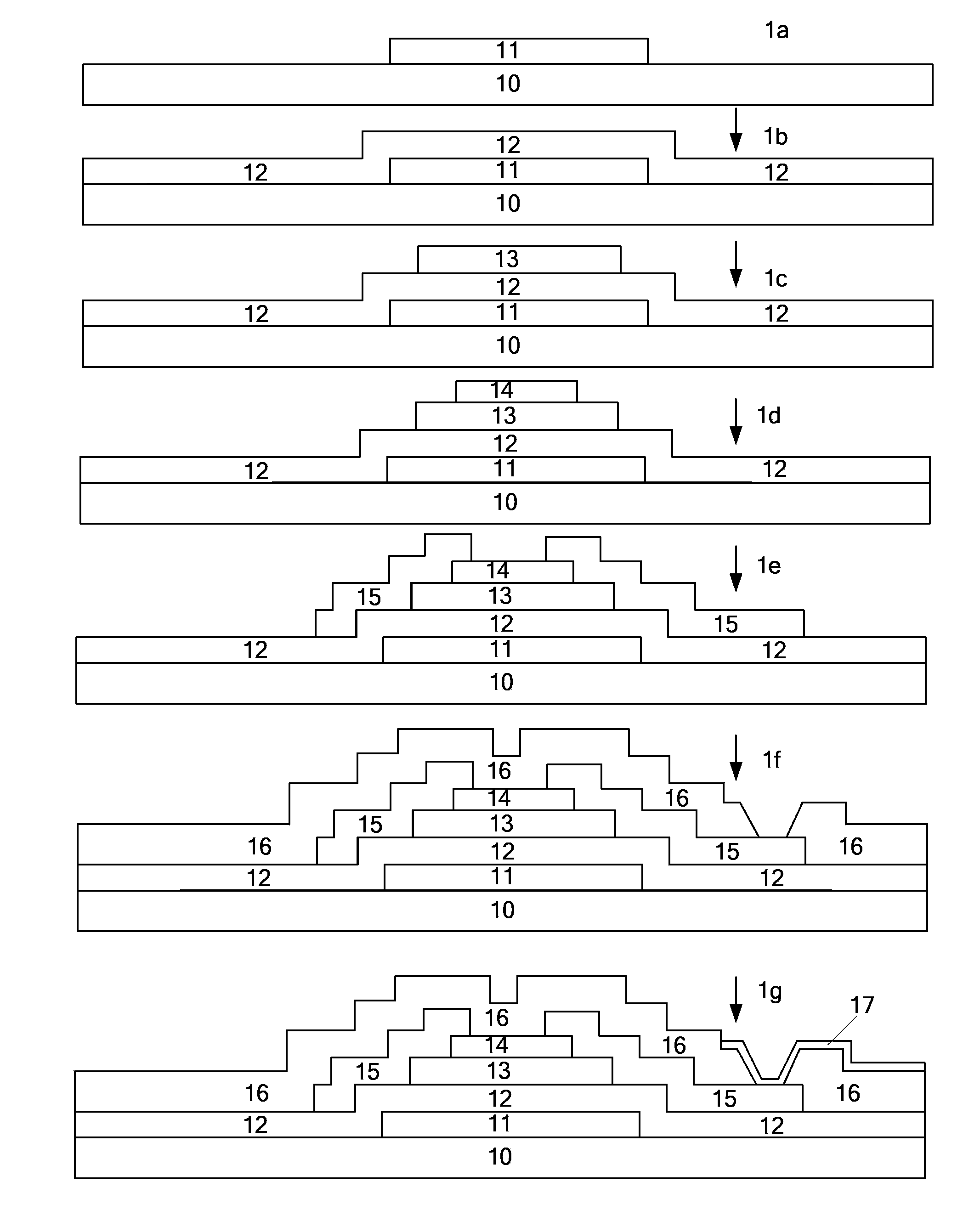
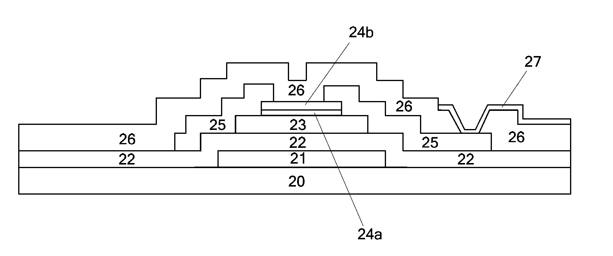
[0055] The basic idea of ​​the present invention is: at least one insulating layer of the thin film transistor is manufactured by a double-layer structure process, that is, the bottom insulating layer and the upper insulating layer are manufactured separately, so that the bottom layer can be made by using different process conditions according to the properties of the insulating layer film. The insulating layer and the upper insulating layer, and the lower insulating layer is used as a barrier layer to make the upper insulating layer, so that the upper insulating layer can be made under the conditions of higher temperature and gas flow than the lower insulating layer, and the characteristics of the insulating layer film are improved. and film deposition rate.

[0056] Taking the etch stop layer in an oxide thin film transistor as an example, the thin film transistor and its manufacturing method of the present invention will be described in detail in combination with specific em...


PUM

PropertyMeasurementUnit
Thicknessaaaaaaaaaa
Thicknessaaaaaaaaaa

Abstract

The invention provides a thin film transistor and a manufacturing method thereof, an array substrate and a display device. The thin film transistor comprises a substrate, a gate electrode, an active layer, a source drain electrode, a pixel electrode and one or more insulation layers, wherein at least one insulation layer comprises a bottom insulation layer and an upper insulation layer, and the content of the hydrogen in the upper insulation layer is higher than the content of the hydrogen in the bottom insulation layer. The thin film transistor is produced by the double-layer etching barrier layer process, the content of the hydrogen in a silicon oxide thin film in an etching barrier layer is effectively reduced, the hydrogen ion generated by silicane decomposition is prevented from reacting with the metal oxide in the active layer, thus the oxide thin film transistor keeps better characteristics, and the thin film deposition rate of the etching barrier layer is increased.

Description

technical field [0001] The invention relates to liquid crystal display technology, in particular to thin film transistor (TFT, Thin Film Transistor) technology in the liquid crystal display technology. Background technique [0002] figure 1 Shows the structure of oxide thin film transistors in the prior art, such as figure 1 As shown, the oxide thin film transistor in the prior art sequentially includes a substrate 10, a gate electrode 11, a gate insulating layer 12, an active layer 13, an etching stopper layer 14, a source-drain electrode 15, a protective layer 16 and a pixel electrode from bottom to top. 17. figure 2 Shows the manufacturing method of the oxide thin film transistor in the prior art, such as figure 2 As shown, in the existing manufacturing method, firstly, the gate electrode 11 is formed on the substrate 10 (such as figure 2 shown in 1a), and then form a gate insulating layer 12 to cover the substrate 10 and the gate electrode 11 (such as figure 2 s...

Claims


Application Information

Patent Timeline
IPC IPC(8): H01L29/786H01L21/336H01L27/12
CPCH01L29/78606H01L29/7869H01L27/1248H01L29/66742H01L27/1225H01L27/1214H01L29/66969G02F1/1368
Inventor 谢振宇徐少颖李田生阎长江李靖田宗民
Owner BEIJING BOE OPTOELECTRONCIS TECH CO LTD
Why Eureka
Try Eureka