Method for production of silicon carbide layer, gallium nitride semiconductor device and silicon substrate

a gallium nitride semiconductor and silicon substrate technology, applied in the direction of chemically reactive gases, crystal growth processes, polycrystalline material growth, etc., can solve the problems of inability to reliably form an upper layer having a uniform crystal shape, inability to promote carbonization satisfactorily and homogeneously on the surface of silicon substrates, and failure to produce an upper layer having a uniform thickness. achieve the effect of avoiding the promotion of unnecessary disintegration of silicon hydrocarbons, stab

Active Publication Date: 2012-07-10
RESONAC CORPORATION
View PDF23 Cites 2 Cited by
  • Summary
  • Abstract
  • Description
  • Claims
  • Application Information

AI Technical Summary

Benefits of technology

[0014]According to the first aspect of the invention, the surface of a silicon substrate heated in high vacuum at a temperature in a range of from 500° C. to 1050° C. is irradiated with a hydrocarbon-based gas as well as an electron beam to form a cubic silicon carbide layer on the silicon substrate surface. Since the electron beam irradiating the surface of the silicon substrate or a growing silicon carbide layer has a function to suppress formation of stacking faults or twin crystals, it is possible to stably produce high-quality cubic silicon carbide layer uniformly coating the silicon substrate surface and having few crystalline defects.
[0015]According to the second aspect of the invention, particularly, in which the substrate surface is irradiated with the hydrocarbon-based gas and electron beam at different angles, promotion of unnecessary disintegration of the silicon hydrocarbon-based gas can be avoided, and deterioration of crystallinity of the silicon carbide layer by ionized fragments can be prevented, thereby enabling a superior-quality silicon carbide layer to be formed.
[0016]According to the third aspect of the invention, particularly, in which the angle of irradiating with the hydrocarbon-based gas is larger than the angle of irradiating with the electron beam in terms of an angle of elevation relative to the surface of the silicon substrate, ionization of the hydrocarbon-based gas by collision with electrons can be suppressed and consequently damage against the silicon carbide layer by the impact of hydrocarbon ions can be reduced, thereby enabling a superior-quality silicon carbide layer to be formed.
[0017]According to the fourth aspect of the invention, particularly, in which the energy beam has an acceleration energy in a range of from 150 eV to 500 eV and a density in a range of from 1×10¹¹ electrons·cm−2 to 5×10¹³ electrons·cm−2, damage of the silicon substrate surface and silicon carbide layer by electrons accelerated under high voltage to have high acceleration energy can be avoided to enable a high-quality silicon carbide layer excellent in crystallinity.

Problems solved by technology

In the prior art means for simply carbonizing the silicon surface, however, the carbonization does not always be promoted satisfactorily homogeneously on the surface of a silicon substrate.
That is to say, a silicon carbide layer having a uniform thickness cannot reliably be formed.
This is problematic.
Even when such a layer inhomogeneous in configuration is used as an under layer, therefore, formation of an upper layer having a uniformly unified crystal shape will fail to produce.
According to the prior art techniques, however, it is impossible as described above to reliably form a silicon carbide layer uniformly coating the entire surface of the silicon substrate.
This is also problematic.

Method used


Image

  • Method for production of silicon carbide layer, gallium nitride semiconductor device and silicon substrate
  • Method for production of silicon carbide layer, gallium nitride semiconductor device and silicon substrate

Examples


Embodiment Construction

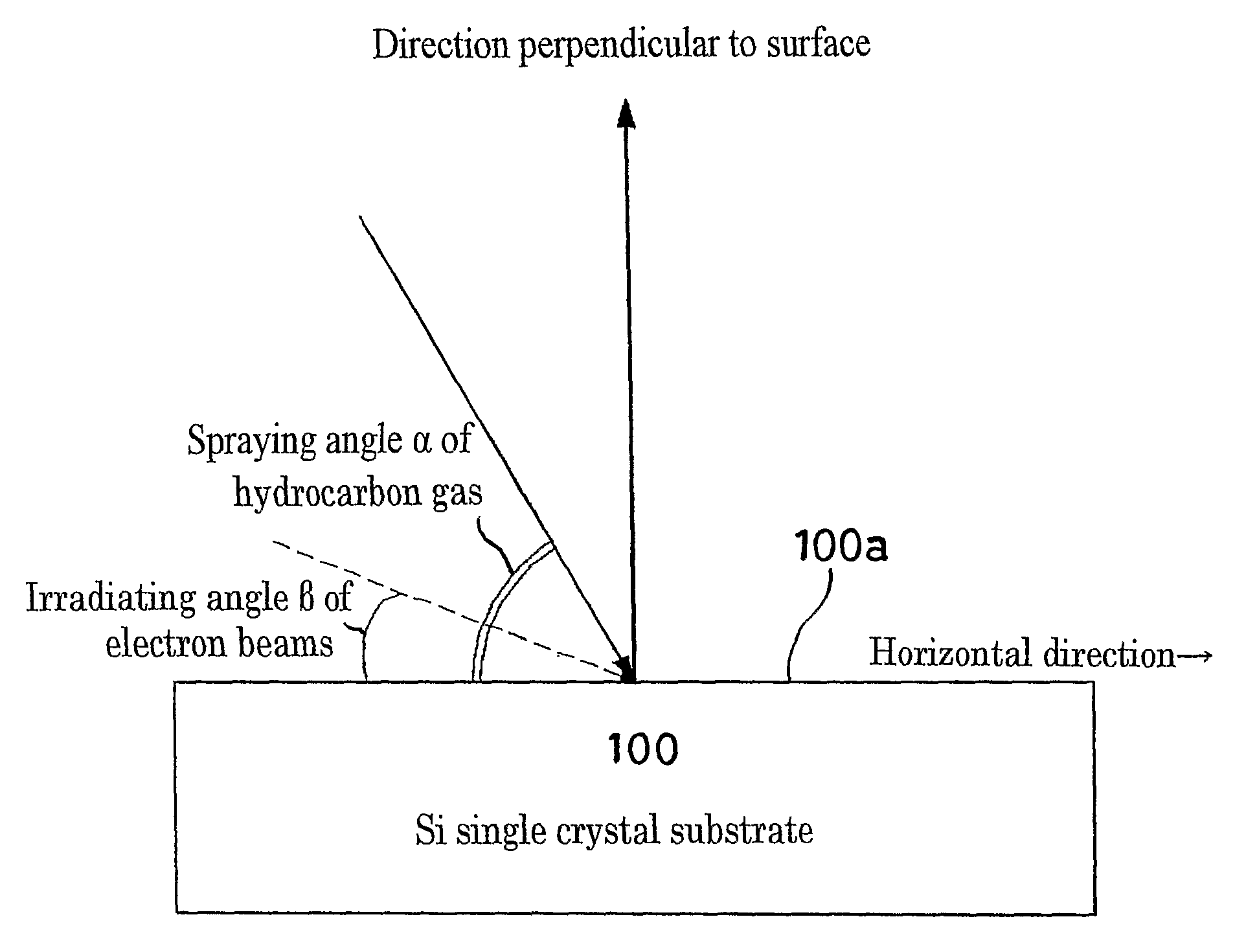
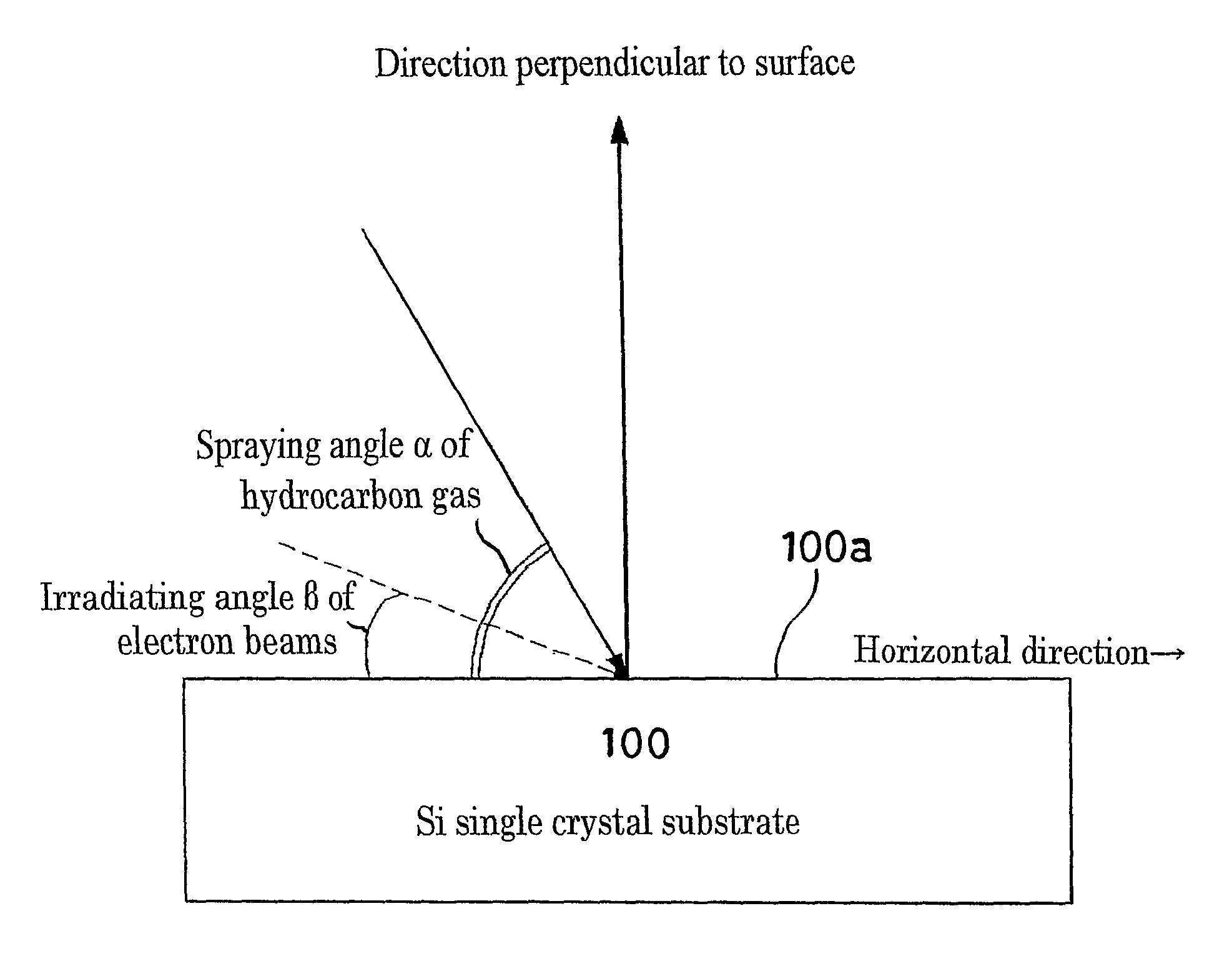
[0020]A cubic silicon carbide crystal layer, particularly 3C-silicon carbide layer (SiC layer) according to the Ramsdell notation, can be formed into a silicon substrate with a surface having various crystal planes (refer to “Electric Refractory Materials,” Marcel Decker, Inc., 2000, pp. 409-411). To form a 3C—SiC layer oriented in the [001] direction, it is advantageous that (001)-silicon with the (001) crystal plane as its surface be used as a substrate. To form a 3C—SiC layer oriented in the [111] direction, (111)-silicon with the (111) crystal plane as its surface is used as a substrate.

[0021]What is advantageously used to form a cubic silicon carbide crystal layer on the surface of a silicon substrate is gaseous hydrocarbon decomposed at low temperatures to produce carbon-containing fragments, which is acetylene (C2H2), for example. The easily decomposable aliphatic hydrocarbon gas is supplied into an MBE apparatus retained in high vacuum via flow rate control equipment capable...


PUM

PropertyMeasurementUnit
temperatureaaaaaaaaaa
lattice spacingaaaaaaaaaa
acceleration energyaaaaaaaaaa

Abstract

A method for producing a silicon carbide layer on a surface of a silicon substrate includes the step of irradiating the surface of the silicon substrate heated in a high vacuum at a temperature in a range of from 500° C. to 1050° C. with a hydrocarbon-based gas as well as an electron beam to form a cubic silicon carbide layer on the silicon substrate surface.

Description

CROSS REFERENCE TO RELATED APPLICATIONS[0001]This application is a §371 of PCT / JP2006 / 310614 filed May 23, 2006, claiming the benefit of Provisional Application No. 60 / 693,095 filed Jun. 23, 2005 and Japanese Patent Application No. 2005-173209 filed Jun. 14, 2005.TECHNICAL FIELD[0002]The present invention relates to a method for producing a silicon carbide layer on the surface of a silicon substrate, to a gallium nitride semiconductor device formed on the silicon carbide layer and to a silicon substrate including the silicon carbide layer.BACKGROUND ART[0003]As technical means for forming silicon carbide (SiC) on the surface of a silicon substrate, there has heretofore been known the Chemical Vapor Deposition (CVD) means using saturated aliphatic hydrocarbons and a homologue of silicon tetrachloride as raw materials. For example, a technique for growing an SiC film on the surface of an Si substrate through the CVD method using propane (C3H8) and trichlorosilane (SiHCl3) as raw mater...

Claims


Application Information

Patent Timeline
Patent Type & Authority Patents(United States)
IPC IPC(8): C30B25/02
CPCC30B25/02C30B29/36H01L21/02381H01L21/02433H01L21/02447H01L21/02529H01L21/0254H01L21/0262H01L21/02631
Inventor UDAGAWA, TAKASHI
Owner RESONAC CORPORATION
Why Eureka
Try Eureka