Method for manufacturing phase change memory device

a memory device and phase change technology, applied in the direction of instruments, sextants, testing food, etc., can solve the problems of flash memory devices that require high operation voltage, flash memory devices that cannot achieve a high level of integration in a dram, and difficulties experienced in flash memory devices, so as to achieve the effect of preventing or preventing

Active Publication Date: 2012-07-10
SK HYNIX INC
View PDF6 Cites 2 Cited by
  • Summary
  • Abstract
  • Description
  • Claims
  • Application Information

AI Technical Summary

Benefits of technology

[0010]Embodiments of the present invention are directed to a method for manufacturing a phase change memory device which can prevent or at least minimize the characteristics of a phase change layer from becoming non-uniform due to composition changes and etch losses of the phase change layer that can arise from inadequate overlap when forming top electrode contacts.

Problems solved by technology

Since the surface area of an electrode must be increased to achieve a high charge storing capacity, it is difficult to achieve a high level of integration in a DRAM.
Further, difficulties are experienced in the flash memory devices because of the fact that flash memory devices often require that two gates are stacked upon each other.
Therefore, flash memory devices require high operation voltages when compared to the power source voltage demands of volatile RAMs.
Accordingly, it is difficult to achieve a high level of integration for flash memory devices.
If the overlap even slightly deviates away from forming the top electrode contacts, the phase change layer zones, which underlies the top electrodes, are likely to be inadvertently etched, and as a result the top electrode contacts can directly contact the phase change layer.
Accordingly, as a result of this scenario of slight misalignment and inadvertent etching of the phase change layer, the electrical performance characteristics of the phase change layer may become non-uniform.
However, in this case, as the size of the cells increases in the direction of word lines, the area of an entire semiconductor chip increases, whereby defeating the goal of achieving a high integration of the phase change memory device.
Alternately, if the top electrode contacts are patterned on the top electrodes to have a decreased size, then the contact resistance between the top electrodes and the bit lines increases, and as a result the current flow from the bit lines to switching elements may change, or non-uniform contacts may be formed so that the bit lines are electrically open relative to the top electrodes.

Method used


Image

  • Method for manufacturing phase change memory device
  • Method for manufacturing phase change memory device
  • Method for manufacturing phase change memory device

Examples


Embodiment Construction

[0028]Hereafter, the specific embodiment of the present invention will be described in detail with reference to the accompanying drawings.

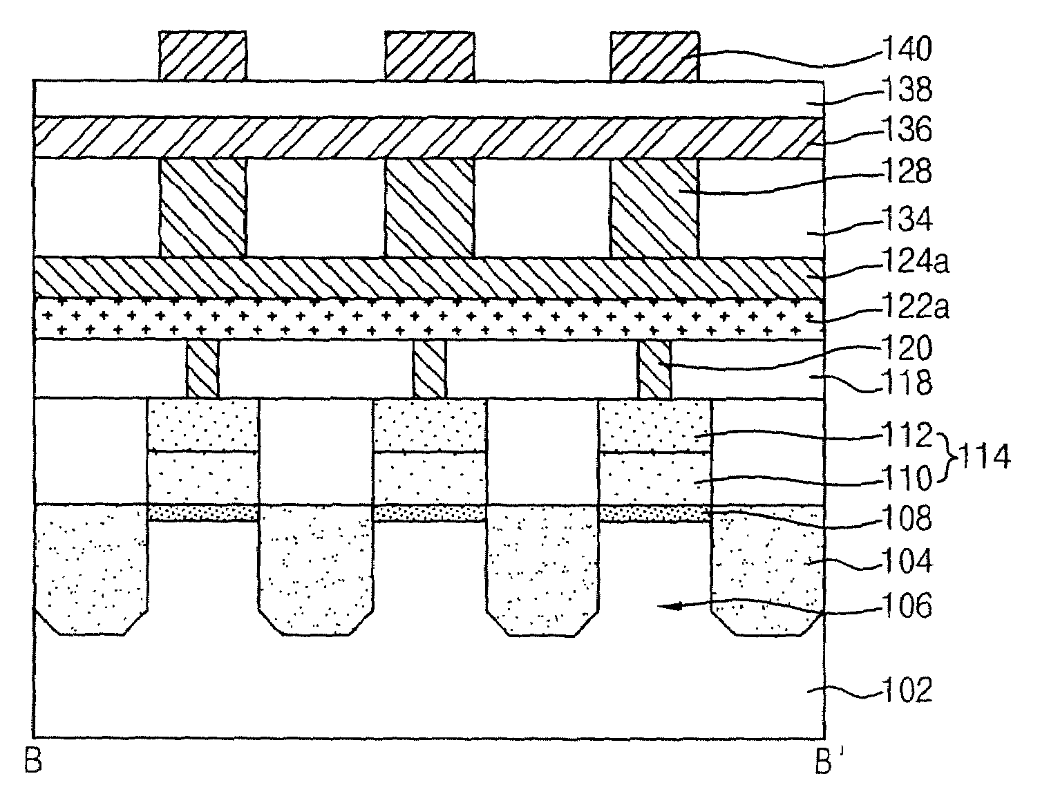
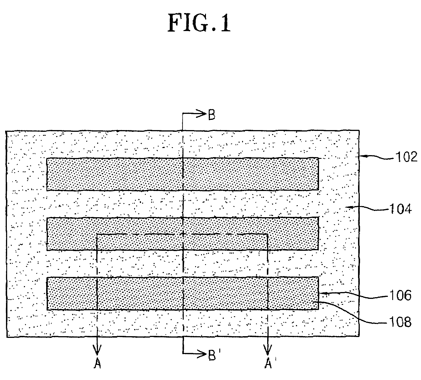
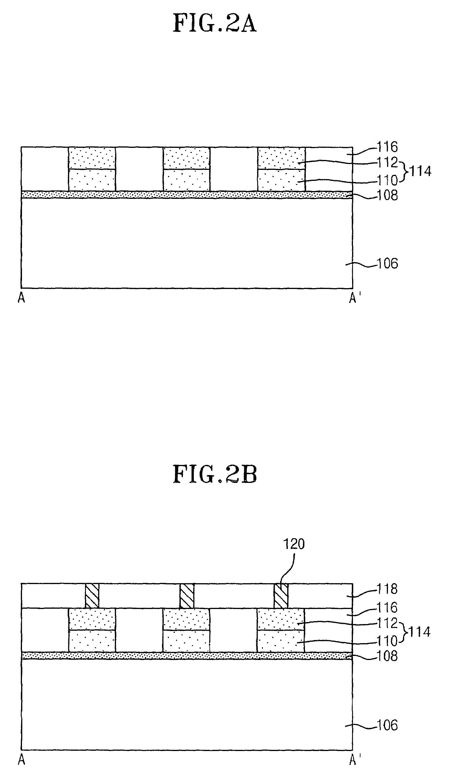
[0029]FIG. 1 is a top plan view used to explain a method for manufacturing a phase change memory device in accordance with an embodiment of the present invention. FIGS. 2A through 2J are cross sectional side views, taken along the line A-A′ of FIG. 1, illustrating some of the processes of the method for manufacturing a phase change memory device in accordance with the embodiment of the present invention. FIGS. 3A through 3J are cross sectional side views, taken along the line B-B′ of FIG. 1, illustrating some of the processes of the method for manufacturing a phase change memory device in accordance with the embodiment of the present invention.

[0030]Referring to FIGS. 2A and 3A, an isolation structure 104 is formed in a semiconductor substrate 102 to delimit active regions 106. By implanting N+ impurities in the surfaces of the active regions 106 ...


PUM


Abstract

A method for manufacturing a phase change memory device that prevents or minimizes adverse performance characteristics associated with inadequate overlap between top electrode contacts and top electrodes. The method prevents or minimizes unwanted chemical changes and etch losses of the phase change material when building the top electrode. The method includes forming spacers on sidewalls of remaining portions of the insulation layer and the hard masks so that subsequent etching of the conductive layer and the phase change material layer uses the spacers and the hard masks as an etch mask to form top electrodes and a phase change layer. Accordingly, the method promises to provide a way of achieving a high level of integration for the resultant phase change memory devices.

Description

CROSS-REFERENCE TO RELATED APPLICATIONS[0001]The present application claims priority to Korean patent application number 10-2008-0039947 filed on Apr. 27, 2008, which is incorporated herein by reference in its entirety.BACKGROUND OF THE INVENTION[0002]The present invention relates generally to a method for manufacturing a phase change memory device, and more particularly to a method for manufacturing a phase change memory device that can form stable top electrode contacts.[0003]Memory devices are largely divided into a volatile RAM (random access memory) sub-category that loses inputted information when power is interrupted and into a non-volatile ROM (read-only memory) sub-category that can continuously maintain the stored state of inputted information even when power is interrupted. As to well-known representative volatile RAMs, DRAMs (dynamic RAM) and SRAMs (static RAM) can be mentioned. As to well known representative non-volatile ROMs, a flash memory device such as the EEPROM (...

Claims


Application Information

Patent Timeline
Patent Type & Authority Patents(United States)
IPC IPC(8): H01L21/302
CPCH01L27/2409H01L27/2463H01L45/06H01L45/1233H01L45/144H01L45/165H01L45/1675H10B63/20H10B63/80H10N70/231H10N70/043H10N70/826H10N70/8828H10N70/063H01L21/31051
Inventor CHANG, HEON YONG
Owner SK HYNIX INC
Why Eureka
Try Eureka