Method of making a trench MOSFET having improved avalanche capability using three masks process

a technology of avalanche capability and three masks, which is applied in the field of cell structure and device configuration of semiconductor devices, can solve the problems of difficult turning, reduced emitter injection efficiency of parasitic npn, etc., and achieves the effects of enhancing contact performance, reducing fabrication costs, and enhancing contact performan

Active Publication Date: 2012-07-17
FORCE MOS TECH CO LTD
View PDF4 Cites 5 Cited by
  • Summary
  • Abstract
  • Description
  • Claims
  • Application Information

AI Technical Summary

Benefits of technology

[0008]Another aspect of the present invention is that, in a preferred embodiments, the dopant of source region is diffused to just reach cell edge, please refer to FIG. 2B for a top view of an N-channel trench MOSFET structure, the dash-dotted line illustrate the area of N+ source region with a doping concentration no less than 1×1019 cm−3. At cell corners, the N region has a lower doping concentration due to the Gaussian-distribution, which is less than 1×1019 cm−3. Therefore, a Source Ballast Resistance (SBR) of said N region exists at cell corners, which reduces the Emitter injection efficiency of the parasitic NPN bipolar transistor, thus rendering it difficult to turn on, avoiding the UIS failure issue and improving the avalanche capability.
[0021]Briefly, in another preferred embodiment, as shown in FIG. 8, the present invention discloses a trench MOSFET with termination area having trenched floating rings. In active area, the structure can be same as that in FIG. 3A, in termination area, a plurality of trenched floating rings are formed from top surface of said body region and extending into said epitaxial layer. By employing said trenched floating rings, the body mask is saved, and on the other hand, the breakdown voltage of device is enhanced. Between said active area and said termination area, a wider trenched gate for gate connection is formed to electrically contact said trenched gate with gate metal via a trenched gate contact. Especially, the width of said trenched gate contact in top BPSG or PSG layer is wider than that in lower portion.

Problems solved by technology

Therefore, a Source Ballast Resistance (SBR) of said N region exists at cell corners, which reduces the Emitter injection efficiency of the parasitic NPN bipolar transistor, thus rendering it difficult to turn on, avoiding the UIS failure issue and improving the avalanche capability.

Method used


Image

  • Method of making a trench MOSFET having improved avalanche capability using three masks process
  • Method of making a trench MOSFET having improved avalanche capability using three masks process
  • Method of making a trench MOSFET having improved avalanche capability using three masks process

Examples


Embodiment Construction

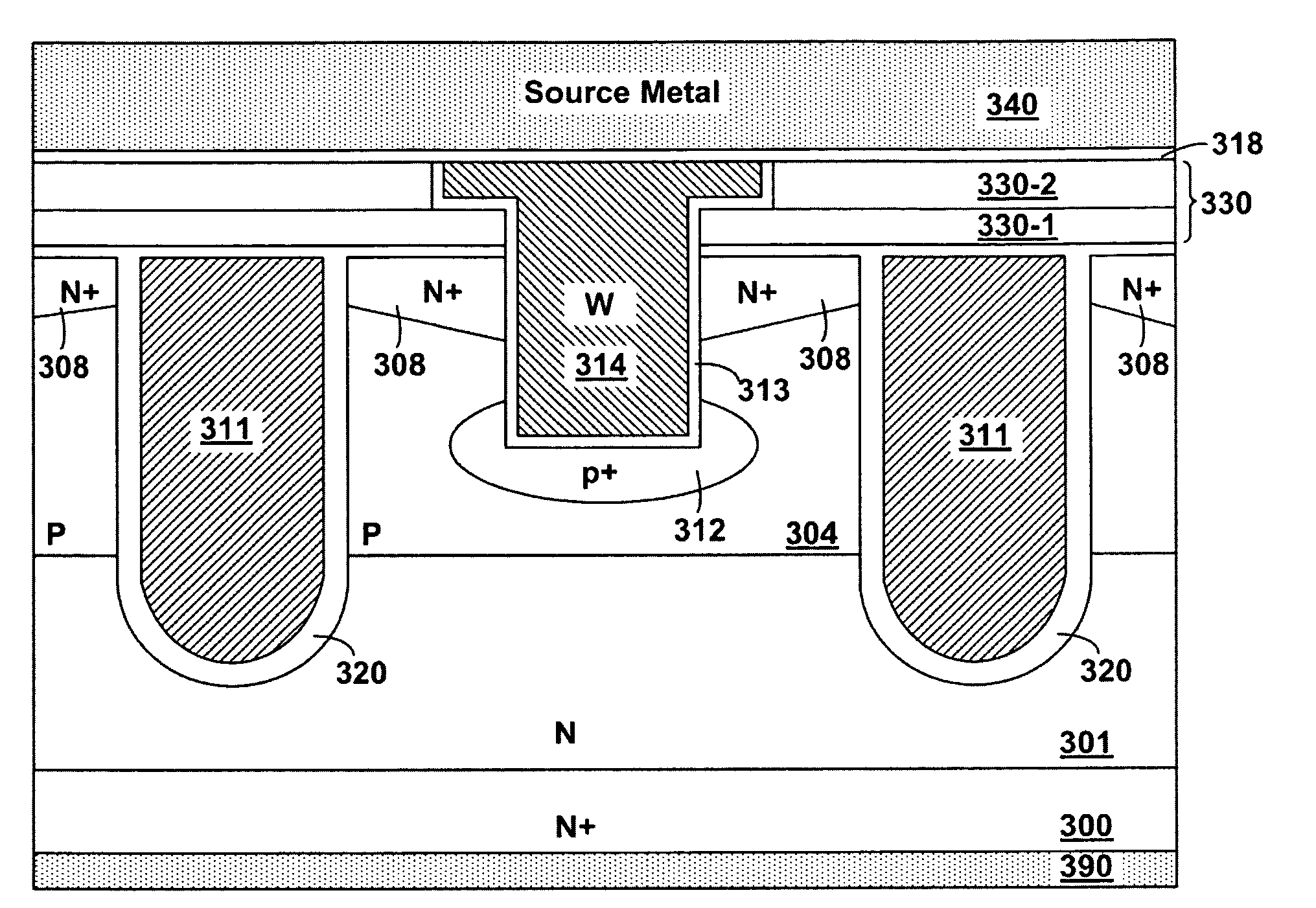
[0041]Please refer to FIG. 3A for a preferred embodiment of the present invention, which also is the X1-X1′ cross section of FIG. 2B and FIG. 2C, where an N-channel trench MOSFET is formed on a heavily N+ doped substrate 300 coated with back metal 390 on rear side as drain electrode. Onto said substrate 300, a lighter N doped epitaxial layer 301 is grown, and a plurality of trenches are etched wherein. Doped poly is filled into these trenches padded with a gate oxide layer 320 to serve as trenched gates 311. P body region 304 is extending between two adjacent trenched gates 311, and near the top surface of said P body region, N+ source regions 308 is formed with Gaussian-distribution from the open region of a thick contact interlayer 330 to channel region. Said thick contact interlayer is composed of a layer of un-doped SRO 330-1 and a layer of BPSG or PSG 330-2. Trenched source-body contact filled with tungsten plug 314 which is padded with a barrier layer 313 of Ti / TiN or Co / TiN, ...


PUM


Abstract

A method of forming trench MOSFET structure having improved avalanche capability is disclosed. In a preferred embodiment according to the present invention, only three masks are needed in the fabricating process, wherein the source region is formed by performing source Ion Implantation through contact open region of a thick contact interlayer for saving source mask. Furthermore, said source region has a doping concentration along channel region lower than along contact trench region, and source junction depth along channel region shallower than along contact trench, and source doping profile along surface of epitaxial layer has Guassian-distribution from trenched source -body contact to channel region.

Description

FIELD OF THE INVENTION[0001]This invention relates generally to the cell structure and device configuration of semiconductor devices. More particularly, this invention relates to an improved trenched MOSFET configuration having improved avalanche capability by three masks process.BACKGROUND OF THE INVENTION[0002]Please refer to FIG. 1A for a conventional N-channel trench MOSFET structure of prior art (U.S. Pat. No. 6,888,196) with an N+ source regions having same surface doping concentration and junction depth along trenched source-body contact and channel region. The disclosed N-channel trench MOSFET cell is formed in an N epitaxial layer 102 supported on an N+ substrate 100. Near the top surface of a P body region 103, which is formed within said epitaxial layer 102, N+ source region 104 is implanted around the top portion of trenched gates 105 and adjacent to the sidewalls of trenched source-body contact 106. As mentioned above, said N+ source region 104 has a same surface doping...

Claims


Application Information

Patent Timeline
Patent Type & Authority Patents(United States)
IPC IPC(8): H01L21/336
CPCH01L29/0696H01L29/086H01L29/66727H01L29/66734H01L29/7811H01L29/7813H01L29/0869H01L29/1095H01L29/407H01L29/41766H01L29/4236H01L29/456
Inventor HSIEH, FU-YUAN
Owner FORCE MOS TECH CO LTD
Why Eureka
Try Eureka