Semiconductor device with stop layers and fabrication method using ceria slurry

a technology of semiconductor/solid-state device and stop layer, which is applied in the direction of semiconductor/solid-state device manufacturing, basic electric elements, electric devices, etc., can solve the problems of difficulty in the formation of minute patterns and misalignment of focus, and achieve excellent planarization and excellent planarization. , excellent planarization

Active Publication Date: 2012-07-17
MONTEREY RES LLC
View PDF12 Cites 0 Cited by
  • Summary
  • Abstract
  • Description
  • Claims
  • Application Information

AI Technical Summary

Benefits of technology

[0012]According to a first aspect of the present invention, there is preferably provided a method of fabricating a semiconductor device including: forming stop layers that include silicon oxy-nitride films above a semiconductor substrate; forming a cover film between and on the stop layers, in which a top surface of the cover film above a region between the stop layers is higher than top surfaces of the stop layers; and polishing the cover film to the stop layers by using ceria slurry. According to the present invention, it is possible to obtaining the film having a surface of excellent planarization.
[0013]According to a second aspect of the present invention, there is preferably provided a method of fabricating a semiconductor device including: forming a first interlayer insulating film above a semiconductor substrate; forming a first layer that includes wiring layers partially above the first interlayer insulating film; forming a cover film between and on the first layers, so that a top surface of the cover film above a region between stop layers is higher than top surfaces of the first layers; forming an embedded layer between the first layers, by polishing the cover film to the first layers; and forming a second interlayer insulating film on the first layers. According to the present invention, after the cover layer is polished to the first layer and planarized, the second interlayer insulating film can be formed. It is therefore possible to offer the second interlayer insulating film having a surface of excellent planarization. Accordingly, the second interlayer insulating film is capable of having a surface of excellent planarization. This makes it possible to miniaturize the wiring on an upper layer.
[0014]According to a third aspect of the present invention, there is preferably provided a semiconductor device including: metal layers provided above a semiconductor substrate; silicon oxy-nitride films provided on the metal layers; and an embedded layer provided between the metal layers to have a top surface substantially coplanar with top surfaces of the silicon oxy-nitride films. According to the present invention, it is possible to provide a semiconductor device having a film of excellent planarization.
[0015]According to a fourth aspect of the present invention, there is preferably provided a semiconductor device including: a first interlayer insulating film provided above a semiconductor substrate; first layers provided partially on the first interlayer insulating film, the first layers including wiring layers; an embedded layer provided on the first interlayer insulating film between the first layers to have a top surface substantially coplanar with top surfaces of the first layers; and a second interlayer insulating film formed on the first layers and on the buried layer. According to the present invention, it is possible to planarize the surface of the second interlayer insulating film, thereby miniaturizing wiring on an upper layer.

Problems solved by technology

For instance, if poor planarization is provided on a plane on which the lithography process is performed, there will cause problems of misaligned focus, difficulty in the formation of a minute pattern, and the like.

Method used


Image

  • Semiconductor device with stop layers and fabrication method using ceria slurry
  • Semiconductor device with stop layers and fabrication method using ceria slurry
  • Semiconductor device with stop layers and fabrication method using ceria slurry

Examples


first embodiment

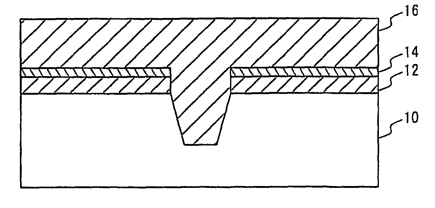
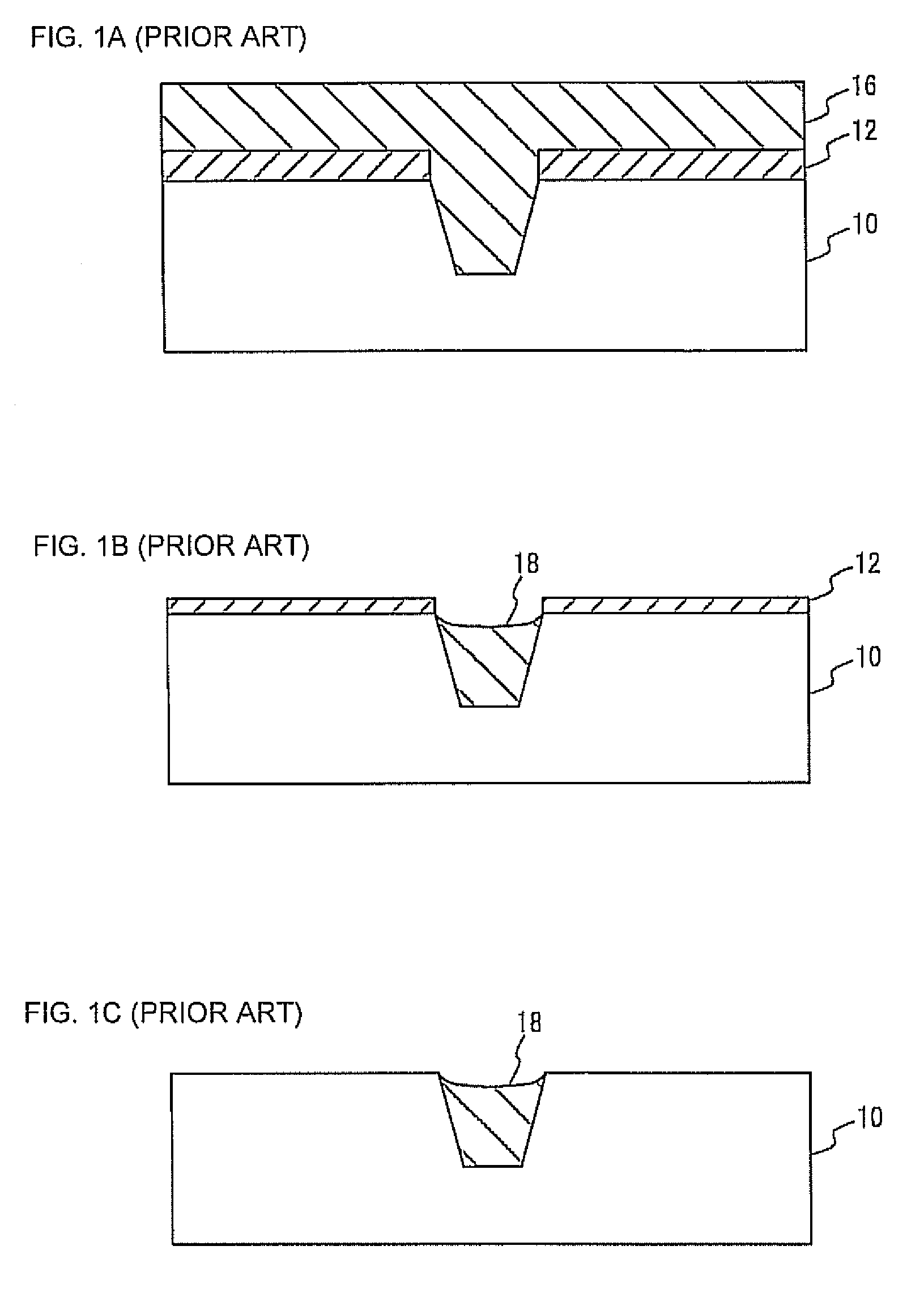
[0031]A first embodiment of the present invention describes an example of forming an embedded silicon oxide film for element isolation and an insulating film is planarized by using a silicon nitride film as a stop layer. FIG. 4A through FIG. 5C are cross-sectional views illustrating a fabrication method of a semiconductor device in accordance with the first embodiment. Referring now to FIG. 4A, a silicon nitride film 12 having a thickness of approximately 100 nm is formed on a silicon substrate 10. On the silicon nitride film 12, a stop layer 14 that includes a silicon oxy-nitride film having a thickness of approximately 35 nm is formed. In one embodiment, this film has a thickness of 10 nm to 50 nm. Referring to FIG. 4B, a photoresist film 20 is applied onto the stop layer 14, and a given region of the photoresist film 20 is exposed with the use of a normal lithography process and then removed during the photoresist development process. The stop layer 14 and the silicon nitride fil...

second embodiment

[0044]A second embodiment describes an example of planarizing a surface of an insulating film formed on a metal layer provided on a substrate. FIG. 9A through FIG. 9D are cross-sectional views illustrating a fabrication method of a semiconductor device in accordance with the second embodiment. Referring now to FIG. 9A, a polysilicon film is formed on the silicon semiconductor substrate 10, as a metal layer. For instance, in a case where the metal layer is used as a gate electrode, an insulating film made of a gate oxide film or the like is formed on the semiconductor substrate 10, and a metal film 31 is formed thereon. The afore-described insulating film is not shown in FIG. 9A through FIG. 9D. A silicon oxy-nitride film 33 to become a stop layer 32 is formed on the metal film 31. In one embodiment, the metal film 31 and the silicon oxy-nitride film 33 respectively have a thickness of approximately 200 nm to 400 nm and a thickness of approximately 10 nm to 50 nm.

[0045]Referring now ...

third embodiment

[0051]A third embodiment describes an example of forming a multilayer wiring on the substrate. FIG. 10A through FIG. 11C are cross-sectional views illustrating a fabrication method of the semiconductor device in accordance with the third embodiment of the present invention. Referring now to FIG. 10A, on the semiconductor substrate 10, wiring layers 50 and a first interlayer insulating film 52 are formed. The wiring layers 50 and the first interlayer insulating film 52 are formed in a similar manner that wiring layers 60 shown in FIG. 10B through FIG. 11C, which will be described later, are replaced by the wiring layers 50 and a second interlayer insulating film 66 and an embedded layer 64 are replaced by the first interlayer insulating film 52, or in a similar manner that the wiring films 60 shown in FIG. 3B and FIG. 3C are replaced by the wiring layers 50 and the first interlayer insulating film 65 are replaced by the first interlayer insulating film 52. The wiring layers 50 mainly...


PUM


Abstract

The present invention provides a method of fabricating a semiconductor device including forming stop layers (32) that include silicon oxy-nitride films above a semiconductor substrate, forming a cover film (34) between and on the stop layers, in which a top surface of the cover film above a region between the stop layers is higher than top surfaces of the stop layers, and polishing the cover film to the stop layers by using ceria slurry, and also provides a semiconductor device including metal layers (30) provided above a semiconductor substrate, silicon oxy-nitride films (32) provided on the metal layers, and an embedded layer (36) provided between the metal layers to have a top surface substantially coplanar with top surfaces of the silicon oxy-nitride films. According to the present invention, it is possible to provide a semiconductor device having a film of excellent planarization on a surface thereof and fabrication method therefor.

Description

CROSS-REFERENCES TO RELATED APPLICATIONS[0001]This is a continuation in part of International Application No. PCT / JP2005 / 011965, filed Jun. 29, 2005 which was not published in English under PCT Article 21(2).BACKGROUND OF THE INVENTION[0002]1. Field of the Invention[0003]This invention relates generally to semiconductors and fabrication methods therefor, and more particularly, to a semiconductor device and a fabrication method therefor with the use of CMP.[0004]2. Description of the Related Art[0005]In order to enhance the performance of semiconductor devices and reduce the costs thereof, development of the layout rule is in progress for the purposes of reducing the size. In this development, planarization technique plays an important role. For instance, if poor planarization is provided on a plane on which the lithography process is performed, there will cause problems of misaligned focus, difficulty in the formation of a minute pattern, and the like. As a representative planarizat...

Claims


Application Information

Patent Timeline
Patent Type & Authority Patents(United States)
IPC IPC(8): H01L21/311
CPCH01L21/3081H01L21/31053H01L21/31111H01L21/32139H01L21/76224
Inventor ENDA, TAKAYUKIMORIYA, MASAYUKI
Owner MONTEREY RES LLC
Why Eureka
Try Eureka