Method and apparatus for a process, voltage, and temperature variation tolerant semiconductor device

a technology of voltage and temperature variation, applied in the field of semiconductor devices, can solve the problems of degrading operating parameters at other process corners, affecting device performance, and affecting device performance, and achieve the effects of reducing the efficiency of the device, and reducing the cost of the devi

Active Publication Date: 2012-07-17
XILINX INC
View PDF23 Cites 25 Cited by
  • Summary
  • Abstract
  • Description
  • Claims
  • Application Information

AI Technical Summary

Benefits of technology

[0008]To overcome limitations in the prior art, and to overcome other limitations that will become apparent upon reading and understanding the present specification, various embodiments of the present invention disclose a method and apparatus to mitigate the effects of process, voltage, and temperature (PVT) variation.

Problems solved by technology

One key challenge presented by deep sub-micron design is the adjustment of the various semiconductor processing steps that are required to implement devices within a silicon die so as to obtain acceptable yield and manufacturability.
While such process adjustments may optimize operating parameters at a particular process corner, the process adjustments may nevertheless produce degraded operating parameters at other process corners.
As a result, process variations that optimize yield and manufacturability may also contribute to detrimental effects on device performance, such as increased leakage current, reduced threshold voltage, and / or increased saturation current.
As geometric features of the deep sub-micron devices continue to shrink, scaling, implant, and annealing process variations invoke increasingly significant device performance degradations.
Voltage and temperature variation, however, may also lead to variations that degrade performance of the semiconductor device over all process, voltage, and temperature (PVT) corners.
As a result, a device that exhibits acceptable performance levels at a first PVT corner, may nevertheless exhibit performance degradations at other PVT corners that are dynamically induced.

Method used


Image

  • Method and apparatus for a process, voltage, and temperature variation tolerant semiconductor device
  • Method and apparatus for a process, voltage, and temperature variation tolerant semiconductor device
  • Method and apparatus for a process, voltage, and temperature variation tolerant semiconductor device

Examples


Embodiment Construction

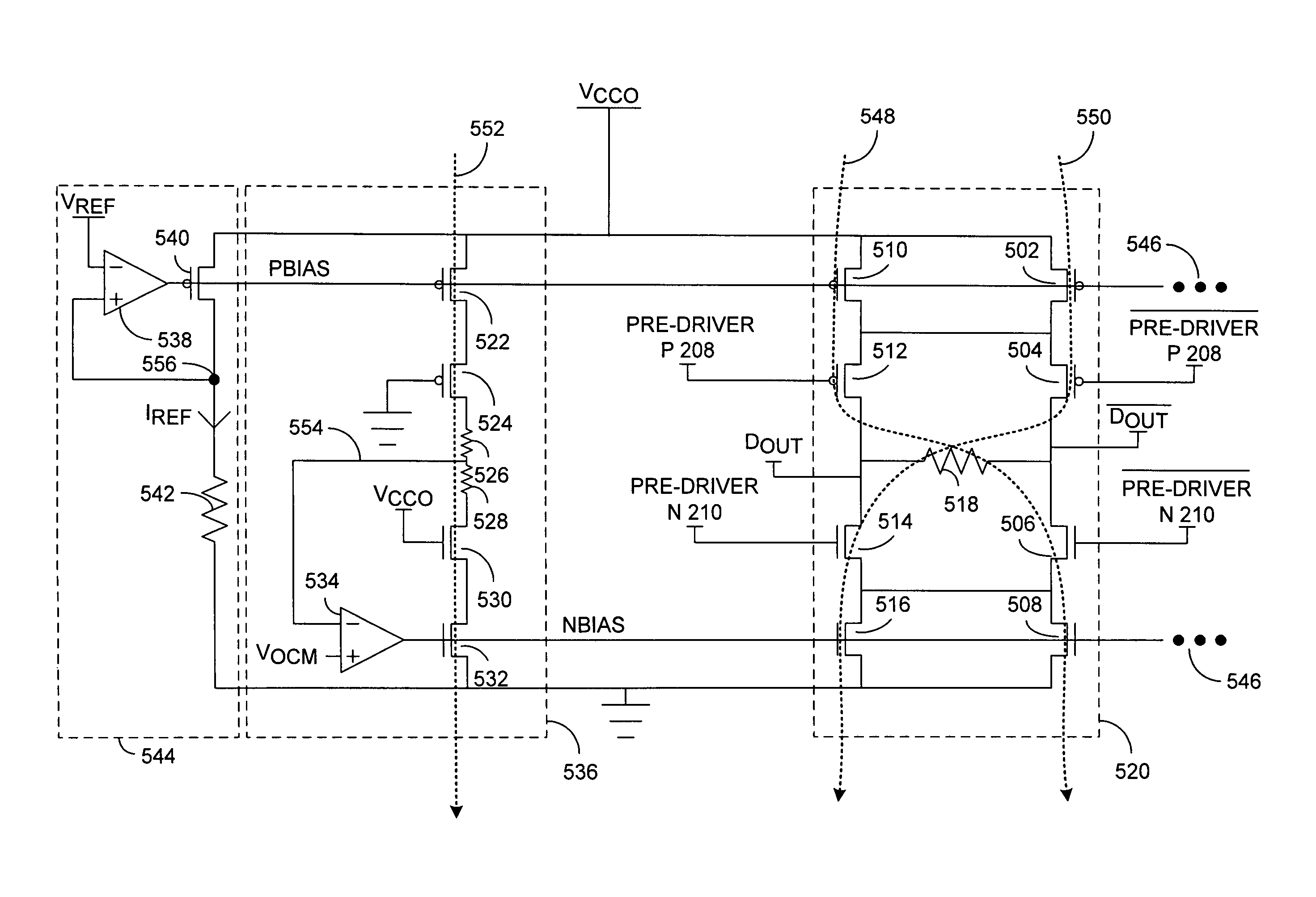
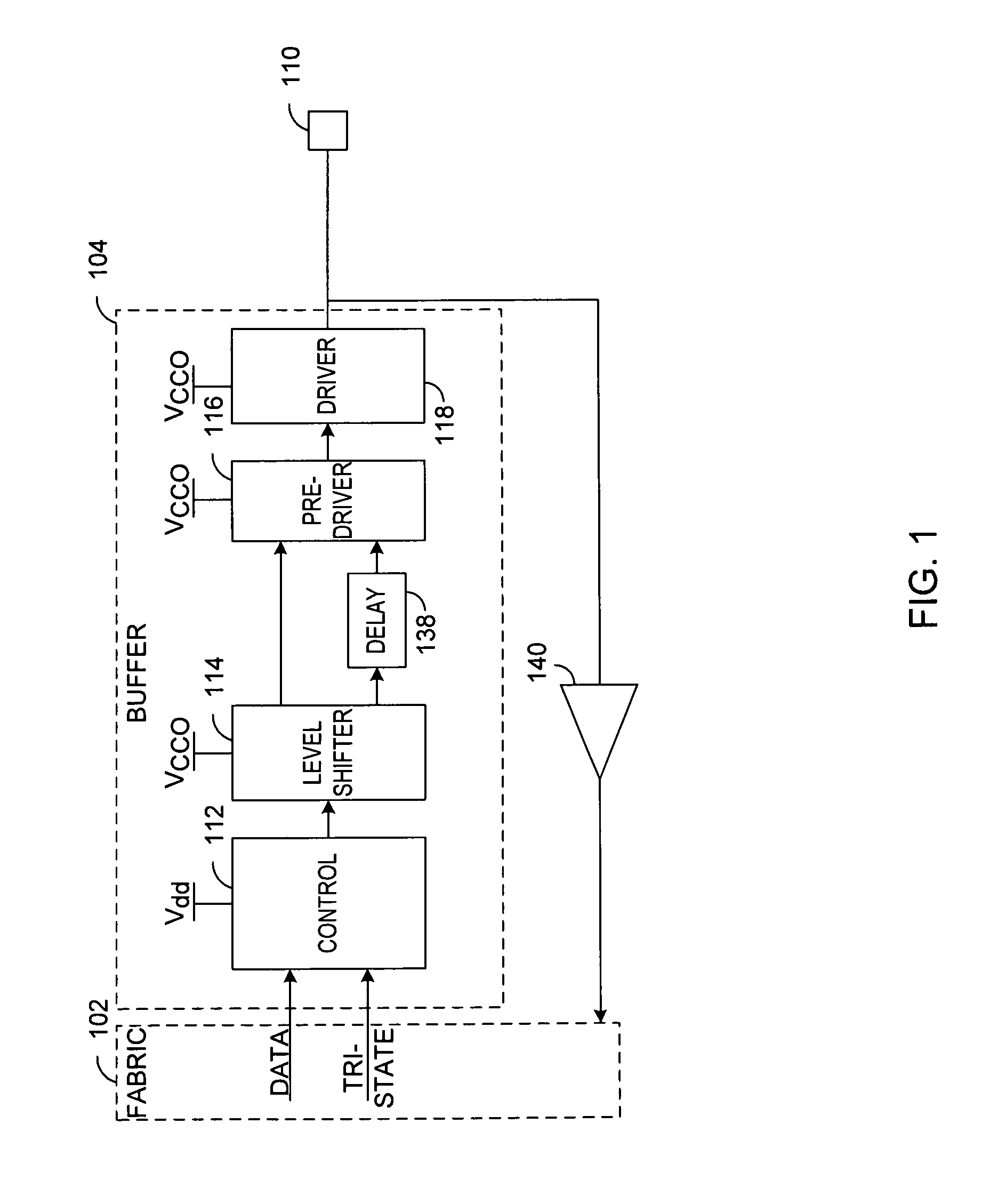
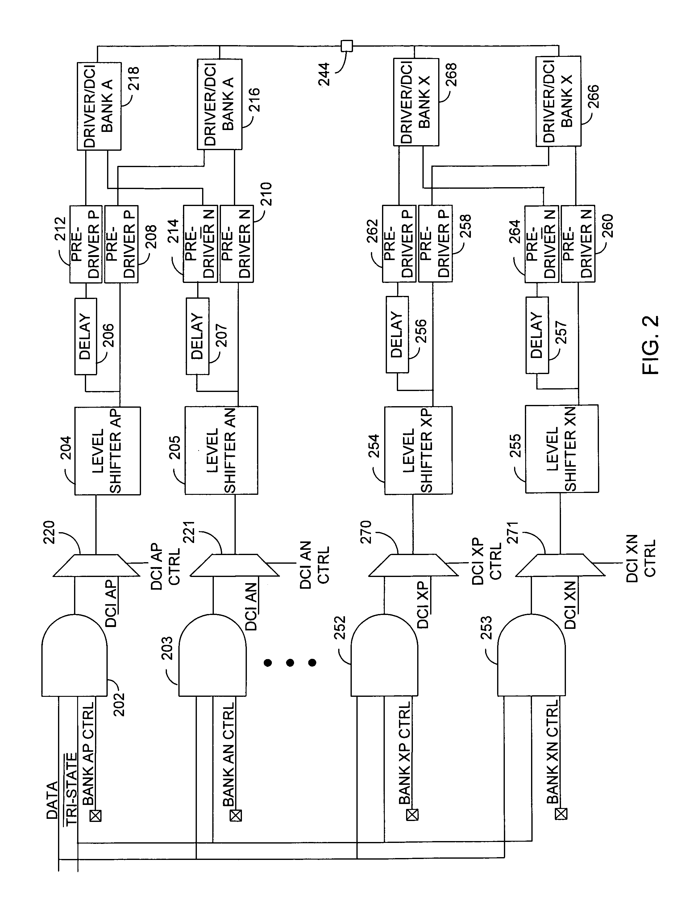
[0020]Generally, various embodiments of the present invention are applied to reduce the degradation in performance of semiconductor-based devices due to process, voltage, and temperature (PVT) and / or other causes of variation. Adaptive feedback mechanisms are employed to sense and correct performance degradation, while simultaneously facilitating configurability that is necessary within integrated circuits (ICs) such as programmable logic devices (PLDs).

[0021]In one embodiment, a voltage-feedback mechanism is employed within a pre-driver of a PLD-based output buffer to detect PVT variation. In response, mirrored current references are adaptively adjusted to track and substantially eliminate the PVT variation. As a result, PVT variation-based slew-rate degradation may be substantially eliminated in accordance with one embodiment of the present invention.

[0022]In an alternate embodiment of the present invention, voltage-feedback mechanisms are utilized to detect PVT-based variations w...


PUM


Abstract

A method and apparatus to reduce the degradation in performance of semiconductor-based devices due to process, voltage, and temperature (PVT) and / or other causes of variation. Adaptive feedback mechanisms are employed to sense and correct performance degradation, while simultaneously facilitating configurability within integrated circuits (ICs) such as programmable logic devices (PLDs). A voltage-feedback mechanism is employed to detect PVT variation and mirrored current references are adaptively adjusted to track and substantially eliminate the PVT variation. More than one voltage-feedback mechanism may instead be utilized to detect PVT-based variations within a differential device, whereby a first voltage-feedback mechanism is utilized to detect common-mode voltage variation and a second voltage-feedback mechanism produces mirrored reference currents to substantially remove the common-mode voltage variation and facilitate symmetrical operation of the differential device.

Description

FIELD OF THE INVENTION[0001]The present invention generally relates to semiconductor devices, and more particularly to semiconductor devices that exhibit performance parameters that are substantially independent of process, voltage, and temperature variation.BACKGROUND OF THE INVENTION[0002]Advances in the field of semiconductor integrated circuits (ICs) have brought about higher levels of integration. Accordingly, semiconductor manufacturing process advancements are driving the corresponding geometric dimensions of semiconductor devices to decreasingly smaller values. 10 micrometer (μm) gate lengths, for example, were common in the 1970's, but continuously advancing semiconductor manufacturing processes have reduced gate lengths to well below 100 nanometers (nm) for deep sub-micron integrated circuit (IC) design.[0003]One key challenge presented by deep sub-micron design is the adjustment of the various semiconductor processing steps that are required to implement devices within a ...

Claims


Application Information

Patent Timeline
Patent Type & Authority Patents(United States)
IPC IPC(8): G05F1/10G05F3/02
CPCH03K19/00369
Inventor REN, GUO JUNZHANG, QISODHA, KETAN
Owner XILINX INC
Why Eureka
Try Eureka