Fabrication process for mastering imaging lens arrays

a technology of imaging lens array and fabrication process, which is applied in the field of fabrication process for mastering large imaging lens array, can solve the problems of wavefront errors, inability to use such techniques for fabricating imaging lenses, and difficulty in ensuring proper quality control using these standard techniques

Active Publication Date: 2012-07-31
FOTONATION LTD
View PDF2 Cites 183 Cited by
  • Summary
  • Abstract
  • Description
  • Claims
  • Application Information

AI Technical Summary

Problems solved by technology

It is not possible to use such techniques for fabricating imaging lenses (such as, e.g., the objectives of mobile phone cameras), which are several orders of magnitude larger, because the magnitude of lens sag is significantly higher, e.g., on the order of hundreds of microns.
As the numbers of individual lens elements required has increased, it has become difficult to ensure proper quality control using these standard techniques.
This shape deviation from the ideal lens profile results in wavefront errors and finally in a reduced image resolution.
In addition, it is difficult to maintain pitch control (i.e., the relative placement of lenses in the x-y plane) when performing such manufacturing across an entire wafer of lens elements.
The result is that it is very difficult to manufacture a master lens array that is close to ideal, i.e., that has properly shaped lenses (no shape deviation), and that are also properly positioned in relation to the other lens elements (good pitch accuracy.
Current manufacturing techniques provide no alternative but to individually diamond turn each of the unique lens elements, which, again, increases the probability that non-ideal master arrays will be formed, i.e., that include one or more shape or pitch deviations.

Method used


Image

  • Fabrication process for mastering imaging lens arrays
  • Fabrication process for mastering imaging lens arrays
  • Fabrication process for mastering imaging lens arrays

Examples


first embodiment

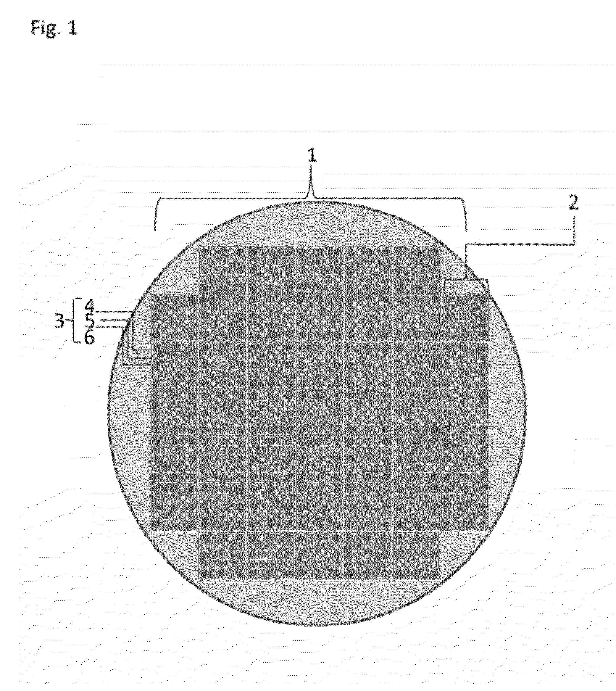
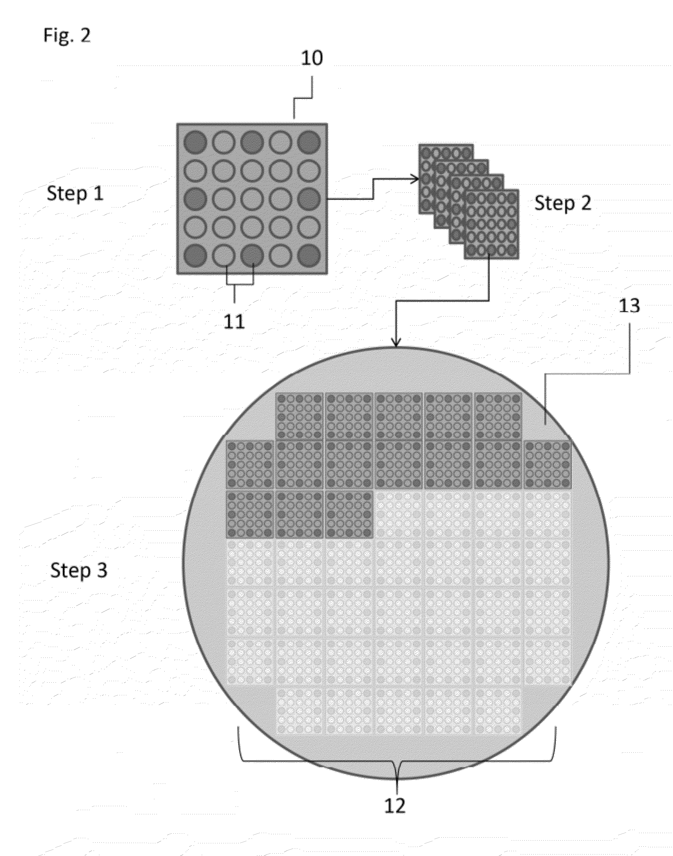
[0030]the invention is shown schematically in FIG. 2. In this embodiment, a sub-array (10) of individual lens elements (11) is formed first and then this sub-array is duplicated across the entire substrate wafer (12) to form the final waferscale lens array (13). More specifically, in a first step each of the lens elements (11) in a sub-array (10), in this case an array of 5×5 individual lens elements, is formed via a conventional manufacturing technique, such as, for example, diamond turning. In a second step this sub-array (10) is quality checked to ensure that each of the individual lens elements has been produced with the correct surface profile and has been positioned properly in relation to the other lens elements. In step 3, once the sub-array has been checked, it is then used as a master to reproduce identical copies of the sub-array across the entire substrate to form the full master array (13). In this embodiment, because the requirement for xy-precision is shifted to that ...

second embodiment

[0032]In a second embodiment, shown schematically in FIG. 3, individual master lens pins are formed. The lens pins can be either single lens elements (20), each having different surface profiles, or small arrays of lens pins (21 to 23) having the same surface profiles. (Step 1) Then, in a second step, these master lens pins are repeatedly used to manufacture the desired lens profile at the right position on the wafer (i.e., in the correct channel of a particular later camera array). Once all the lenses of a first lens pin are reproduced on the entire master array (24) (e.g., for the embodiment shown, 4 times for each sub-array on the wafer), then the pin would be changed and a second lens pin would be used to reproduce all the lenses of the second lens profile, and so on.

[0033]The advantage of this method is that all lenses intended to be identical are identical since they come from the same master pin. Moreover, this pin can be quality checked and iterated in the diamond turning ma...

third embodiment

[0034]the invention (shown schematically in FIG. 4) combines the two approaches set forth above to form a hybrid technique that takes advantage of quality control aspects of both of the earlier fabrication techniques. Specifically, in a first step of this process each of the different lens profiles (30 to 32) would be fabricated (i.e., by diamond turning) as pins once and independently from another. In a second step, these pins (30 to 32) would be used to form a sub-array (33) as in the exemplary embodiment set forth in FIG. 2. For example, in the schematic provided in FIG. 4, three different lens types exchange pins (30 to 32) are formed once by diamond turning. These pins are then used in a Step & Repeat process to form each of the lenses of that type, but only for a sub-array, e.g., in this case a 5×5 array, not the entire master array as proposed in the technique discussed in relation to FIG. 3. This final sub-array (33) can then be quality checked, and, when judged to be good e...


PUM

PropertyMeasurementUnit
radius of curvatureaaaaaaaaaa
shapeaaaaaaaaaa
surface tensionaaaaaaaaaa

Abstract

A process and method for fabricating a master lens array for use in the manufacture of duplicate lens arrays is provided. The fabrication methods provided herein are capable of maximizing the quality of the master lens array in an efficient and cost effective manner, thereby reducing the propagation of errors in the lenses formed using the master lens array.

Description

RELATED APPLICATION[0001]This application claims priority to U.S. Provisional Patent Application 61 / 314,776 filed Mar. 17, 2010, the disclosure of which is hereby incorporated by reference in its entirety.FIELD OF THE INVENTION[0002]The present invention relates to a fabrication process for mastering large imaging lens arrays, which cannot be fabricated by lithographic means.BACKGROUND OF THE INVENTION[0003]The manufacture of very small lenses has undergone enormous development since the 17th century when Robert Hooke and Antonie van Leeuwenhoek both developed techniques to make small glass lenses for use with their microscopes. In these early techniques, Hooke painstakingly melted small filaments of glass and allowed the surface tension in the molten glass to form the smooth spherical surfaces required for lenses. (See, Hooke R, Preface to Micrographia, The Royal. Society of London (1665), the disclosure of which is incorporated herein by reference.)[0004]Advances in technology hav...

Claims


Application Information

Patent Timeline
Patent Type & Authority Patents(United States)
IPC IPC(8): B29D11/00
CPCG02B3/0025Y10T29/49764Y10S425/808B29D11/00346G02B13/02
Inventor DUPARRE, JACQUES
Owner FOTONATION LTD
Why Eureka
Try Eureka