Semiconductor device
a technology of semiconductor devices and semiconductor devices, applied in semiconductor devices, instruments, computing, etc., can solve problems such as easy breakage of ic tags, and achieve the effects of preventing the malfunction of integrated circuits due to stress, improving the stiffness of semiconductor devices, and reducing the risk of bending stress
- Summary
- Abstract
- Description
- Claims
- Application Information
AI Technical Summary
Benefits of technology
Problems solved by technology
Method used
Image
Examples
embodiment 1
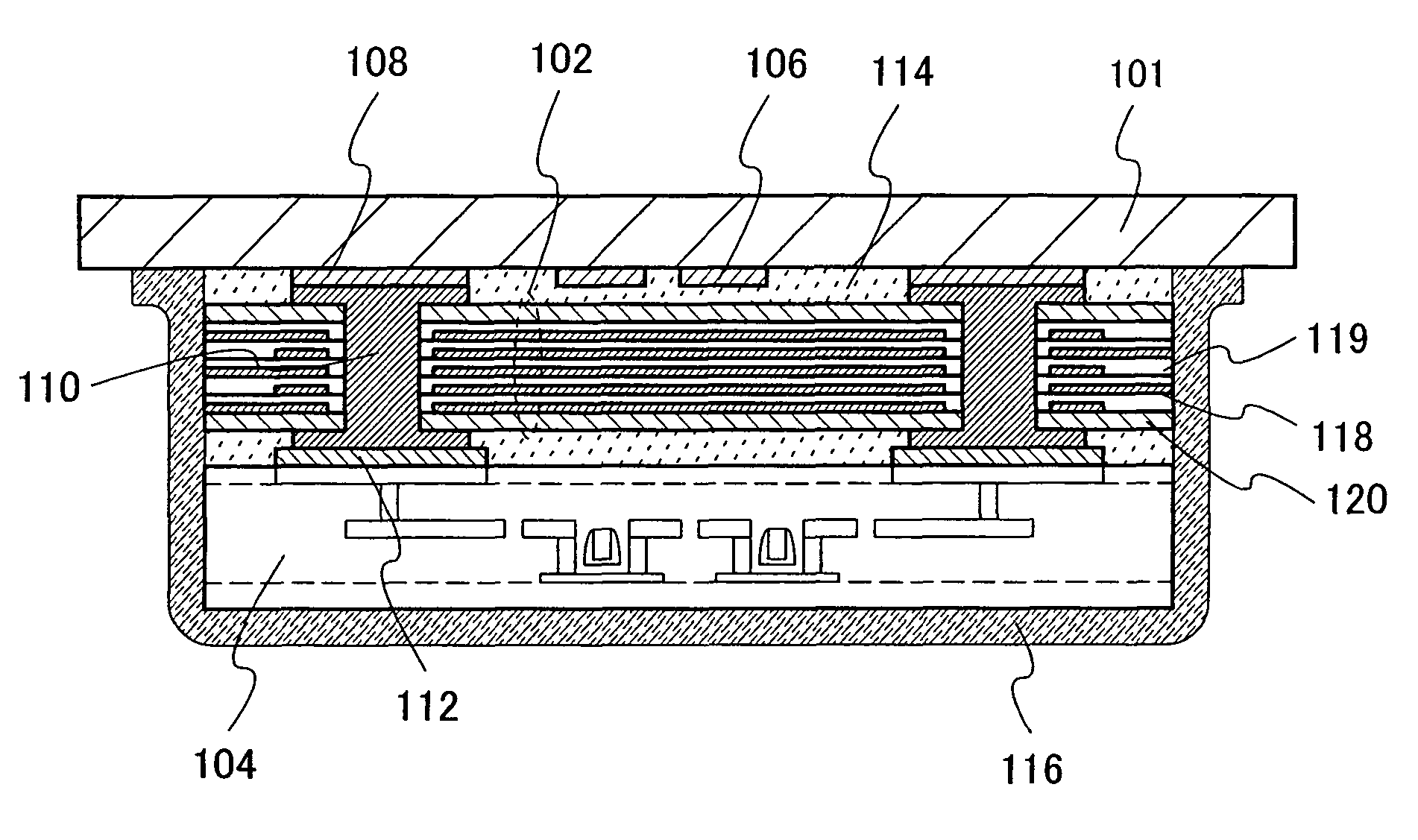
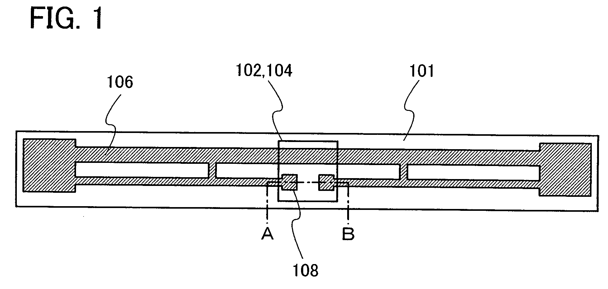
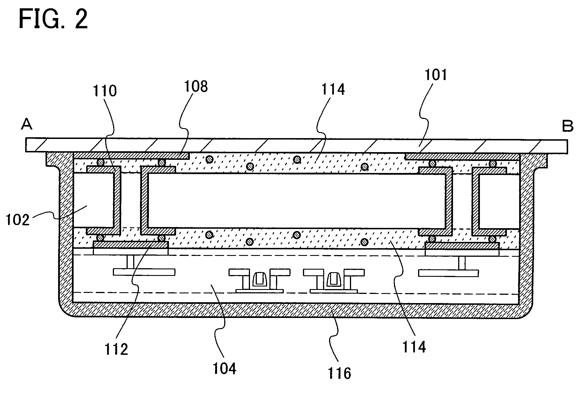
[0049]In this embodiment, one example of a semiconductor device in which a first structural body provided with an antenna, a second structural body provided with a capacitor portion, and an integrated circuit are combined is described with reference to FIGS. 5A to 6B. Note that FIGS. 5A to 5C are plan views showing the semiconductor device, and FIGS. 6A and 6B are cross-sectional views taken along lines A-B and C-D, respectively.
[0050]FIG. 5A shows a mode in which the antenna 106 having a coil-shape is formed in the first structural body 101. The first structural body 101 is formed of a plastic material such as PET (poly ethylene terephthalate), PEN (polyethylene naphthalate), PES (polyethersulfone), polypropylene, polypropylene sulfide, polycarbonate, polyether imide, polyphenylene sulfide, polyphenylene oxide, polysulfone, polyphthalamide, acrylic, or polyimide, or an insulating material such as nonwoven fabric or paper.
[0051]The antenna 106 is formed using a low resistant metal m...
embodiment 2
[0059]In this embodiment, one example of a semiconductor device including a first structural body provided with an antenna, a second structural body provided with a capacitor portion, an integrated circuit, and a ceramic antenna 122 is described with reference to FIGS. 7A to 8B. Note that FIGS. 7A to 7C are plan views showing the semiconductor device, and FIGS. 8A and 8B are cross-sectional views taken along lines E-F and G-H, respectively.
[0060]In FIG. 7A, the antenna 106 having a coil-shape is formed in the first structural body 101. The shape of the antenna 106 may be appropriately set in accordance with a wavelength which is used for communication, as in Embodiment 1.
[0061]FIG. 7A shows a structure in which the second structural body 102, the integrated circuit 104, and the ceramic antenna 122 are provided in accordance with the antenna terminal 108. FIG. 7B shows a plan view of the second structural body 102, FIG. 7C shows a plan view of the integrated circuit 104, and FIG. 7D ...
embodiment 3
[0067]In this embodiment, an example of a semiconductor device which includes a booster coil in order to increase a communication distance is described with reference to FIGS. 9A to 10B. A semiconductor device of this embodiment has an integrated circuit provided with a first antenna, a second structural body provided with a second antenna which is electromagnetically coupled with the first antenna, and a first structural body provided with a third antenna which is electromagnetically coupled with a reader / writer. Note that FIGS. 9A to 9C are plan views showing the semiconductor device, and FIGS. 10A and 10B are cross-sectional views taken along lines J-K and L-M, respectively.
[0068]In FIG. 9A, a third antenna 105 which is electromagnetically coupled with a reader / writer is formed in the first structural body 101. The third antenna 105 is formed, as in Embodiment 1.
[0069]The second structural body 102 and the integrated circuit 104 are provided in accordance with the antenna termina...
PUM
 Abstract
Description
Claims
Application Information


