Light-emitting heat treatment apparatus

a heat treatment apparatus and light-emitting technology, applied in lighting and heating apparatus, instruments, furniture, etc., can solve the problems of non-uniform in-plane temperature distribution in the wafer, affecting the formation of good devices, and essentially non-uniform inner wall surface of the chamber, so as to improve the uniformity prevent the temperature measurement part from suffering, and improve the effect of in-plane temperature distribution

Active Publication Date: 2012-08-07
DAINIPPON SCREEN MTG CO LTD
View PDF28 Cites 4 Cited by
  • Summary
  • Abstract
  • Description
  • Claims
  • Application Information

AI Technical Summary

Benefits of technology

[0012]Since the annular recessed portion with a greater width in a vertical direction than the transport opening is horizontally formed in the inner wall surface of the chamber to surround the periphery of the holding part, and the transport opening communicates with the outer peripheral surface of the recessed portion, there exists no light-reflecting wall surface around the entire circumference of the holding part. This prevents light from being non-uniformly reflected off the inner wall surface of the chamber to enter a substrate, thus improving the uniformity of the in-plane temperature distribution in the substrate during heat treatment.
[0014]The two reflecting barrier plates can be removed for maintenance to ease the operation.
[0016]This allows more light emitted from the first and second light-irradiation parts to enter the peripheral portion of a substrate where a temperature decrease due to heat radiation is likely to occur, thus further improving the uniformity of the in-plane temperature distribution in the substrate during heat treatment.
[0018]Since the retracted positions of the transfer arms of the transfer part are situated within the interior space of the recessed portion, the transfer arms will never obstruct the light emission. This further improves the uniformity of the in-plane temperature distribution in the substrate during heat treatment.
[0020]Since the temperature measurement part is provided within the interior space of the recessed portion, it will never obstruct the light emission. This further improves the uniformity of the in-plane temperature distribution in the substrate during heat treatment and prevents the temperature measurement part from suffering damage from the light emission.
[0021]It is therefore an object of the invention to improve the uniformity of the in-plane temperature distribution in a substrate during heat treatment.

Problems solved by technology

The occurrence of such a phenomenon gives rise to apprehension that the junction may become deeper than the desired level, hindering good device formation.
Thus, if the inner wall surface of the chamber is non-uniform along the circumference of the semiconductor wafer, the reflected light entering the semiconductor wafer becomes non-uniform, which results in a non-uniform in-plane temperature distribution in the wafer.
It is, however, an absolute necessity for the chamber to have a transport opening for transporting a semiconductor wafer therein and thereoutside, so that the inner wall surface of the chamber is essentially non-uniform at the location of the transport opening.
This causes another problem that the portion of a semiconductor wafer that is opposed to the transport opening with no side wall will have a lower temperature than the other portion because of a small amount of incident light thereon, which results in a non-uniform in-plane temperature distribution in the semiconductor wafer.

Method used


Image

  • Light-emitting heat treatment apparatus
  • Light-emitting heat treatment apparatus
  • Light-emitting heat treatment apparatus

Examples


Embodiment Construction

[0031]A preferred embodiment of the present invention is now described in detail with reference to the drawings.

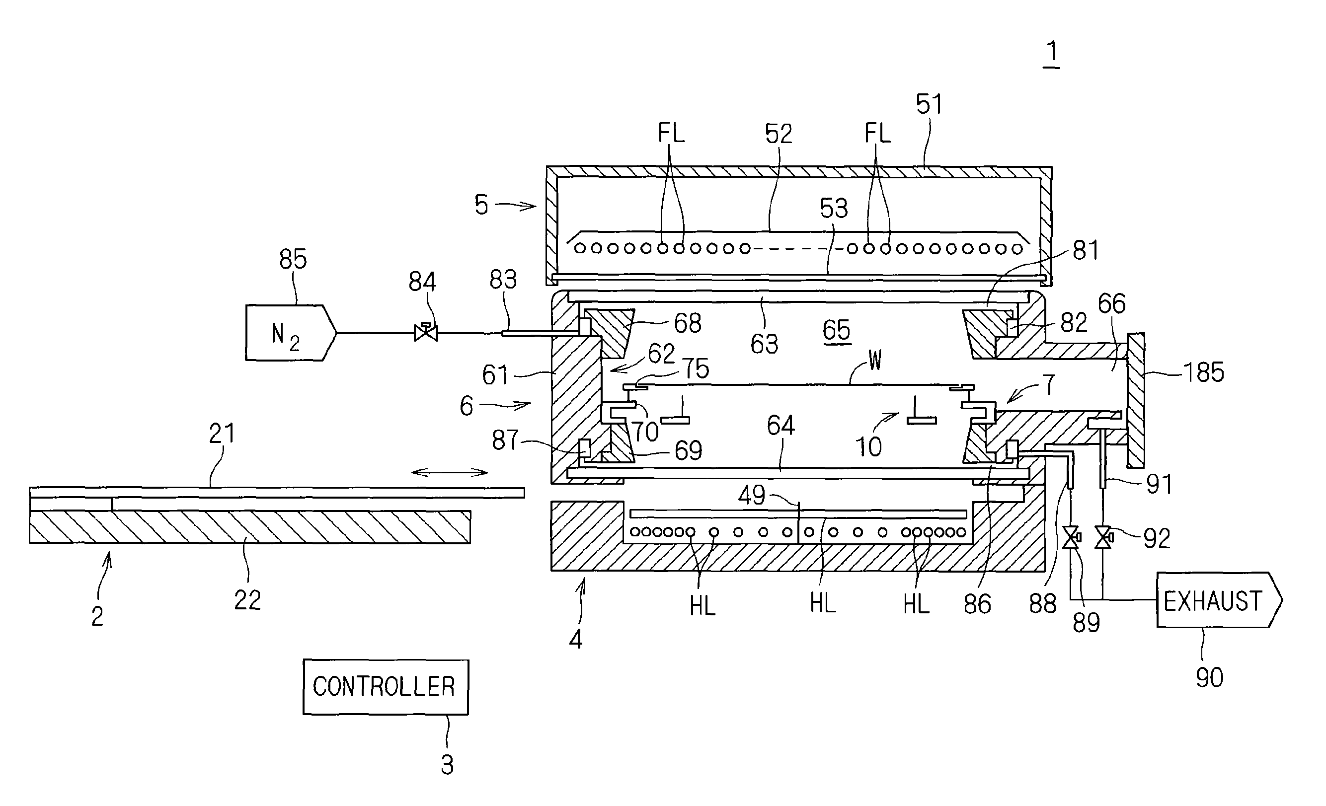
[0032]FIG. 1 is a side sectional view showing the construction of a heat treatment apparatus 1 according to the invention. The heat treatment apparatus 1 according to the present preferred embodiment shall be a flash lamp annealer for heating a 300 mm-diameter disc-shaped semiconductor wafer W serving as a substrate by flash-light irradiation.

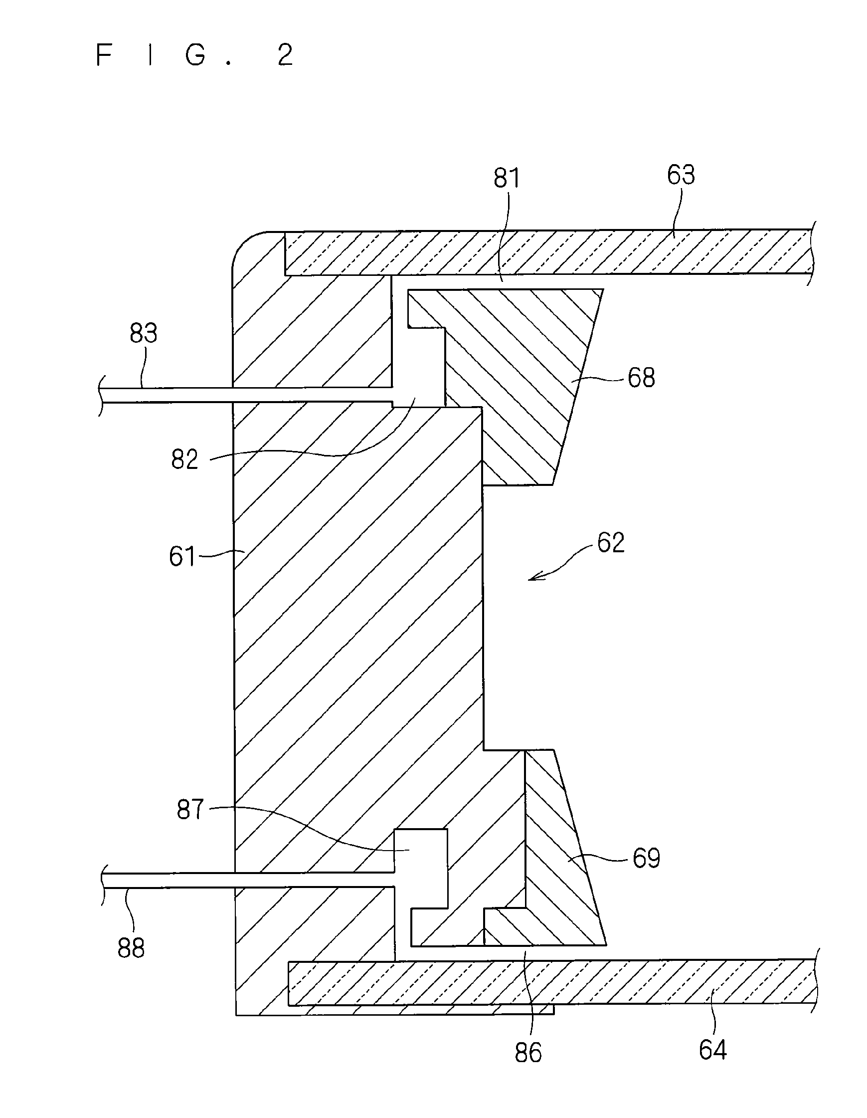
[0033]The heat treatment apparatus 1 includes a chamber 6 for receiving a semiconductor wafer W therein; a flash heating part 5 with a plurality of built-in flash lamps FL; a halogen heating part 4 with a plurality of built-in halogen lamps HL; and a shutter mechanism 2. The flash heating part 5 is provided above the chamber 6, and the halogen heating part 4 below the chamber 6. The heat treatment apparatus 1 further includes, inside the chamber 6, a holding part 7 for holding a semiconductor wafer W in a horizontal position; and a tr...


PUM


Abstract

Annular reflecting rings are removably mounted on the upper and lower sides of a chamber side portion of a chamber. An annular recessed portion is formed sandwiched between the lower end face of the upper reflecting ring and the upper end face of the lower reflecting ring to surround a holding part for holding a semiconductor wafer. The outer peripheral surface of the recessed portion communicates with a transport opening. The formation of the recessed portion prevents the light emitted from halogen lamps and flash lamps from being non-uniformly reflected around the holding part to enter a semiconductor wafer, thus improving the uniformity of the in-plane temperature distribution in the semiconductor wafer during heat treatment.

Description

BACKGROUND OF THE INVENTION[0001]1. Field of the Invention[0002]The present invention relates to a heat treatment apparatus for heating a semiconductor wafer, a glass substrate, or other substrates by light irradiation.[0003]2. Description of the Background Art[0004]Conventionally, lamp annealers employing halogen lamps have been commonly used in the step of activating ions in a semiconductor wafer after ion implantation. Such lamp annealers carry out the activation of ions in a semiconductor wafer by heating (or annealing) the semiconductor wafer to a temperature of the order of, for example, 1000° C. to 1100° C. Such heat treatment apparatuses utilize the energy of light emitted from halogen lamps to raise the temperature of a substrate at a rate of about several hundred degrees per second.[0005]In recent years, with increasing degree of integration of semiconductor devices, it has been desired that the junction be made shallower with decreasing gate length. It has turned out, how...

Claims


Application Information

Patent Timeline
Patent Type & Authority Patents(United States)
IPC IPC(8): A21B2/00
CPCF27B17/0025H01L21/67115H01L21/67748H01L21/68707
Inventor NAKAJIMA, TOSHIHIRO
Owner DAINIPPON SCREEN MTG CO LTD
Why Eureka
Try Eureka