Method of manufacturing semiconductor device

a manufacturing method and semiconductor technology, applied in the direction of semiconductor devices, basic electric elements, electrical appliances, etc., can solve the problems of non-uniform height of sidewall gate electrodes, partially thinned portions, and difficult control of over-etching, etc., to achieve the effect of suppressing non-uniform depth

Inactive Publication Date: 2012-08-21
LONGITUDE LICENSING LTD
View PDF8 Cites 5 Cited by
  • Summary
  • Abstract
  • Description
  • Claims
  • Application Information

AI Technical Summary

Benefits of technology

[0007]The invention has been made to solve the above problems. An object of the invention is to provide a method capable of forming a sidewall film on a side surface of a trench while suppressing non-uniformity of depths from a trench opening on an upper surface of the sidewall film, without etching-damage on a surface of the sidewall film when forming the sidewall film on the side surface of the trench.
[0028]According to the above exemplary embodiments, when the etching-back is performed so that a height of an upper end of a layer filled in a trench formed on a surface of a semiconductor substrate is lower than an opening of the trench by a predetermined height, it is possible to reduce the non-uniformity of heights in a wafer.
[0029]In addition, when the etching-back is performed so that a height of an upper end of a film formed on the inner walls of the trench formed on the surface of the semiconductor substrate is lower than an opening edge of the trench by a predetermined height, it is possible to reduce the non-uniformity of heights in a wafer and to prevent the film thickness from being reduced due to an over-etching of the film surface.
[0030]In particular, it is possible to control an etching end point, which has been conventionally controlled by time, by a shape of a depression of the film surface formed in the trench in a self-aligned manner.

Problems solved by technology

The over-etching is hardly controllable because the etching is unusually progressed not only on the upper end of the sidewall gate electrodes but also on the side surfaces of the sidewall gate electrodes, so that a partially thinned portion is generated by irregularly progressing side etching or heights of the sidewall gate electrodes become non-uniform.

Method used


Image

  • Method of manufacturing semiconductor device
  • Method of manufacturing semiconductor device
  • Method of manufacturing semiconductor device

Examples


exemplary embodiment 1

[0059]In the followings, a process of manufacturing a semiconductor device according to a first exemplary embodiment will be described.

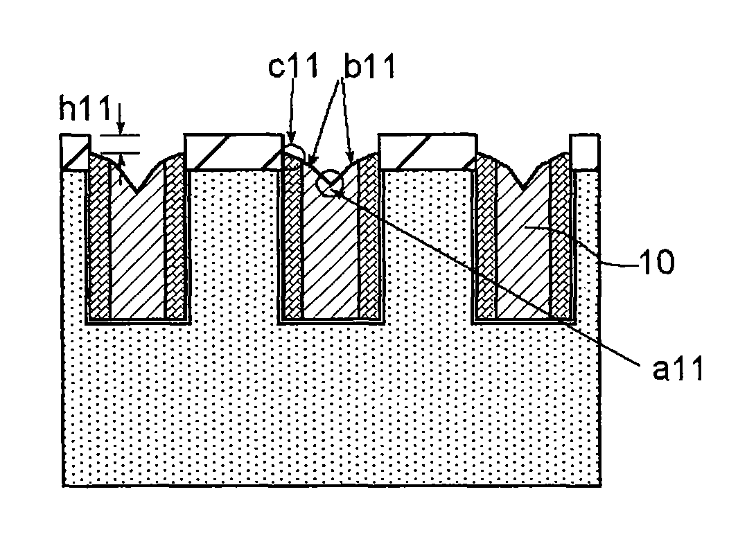
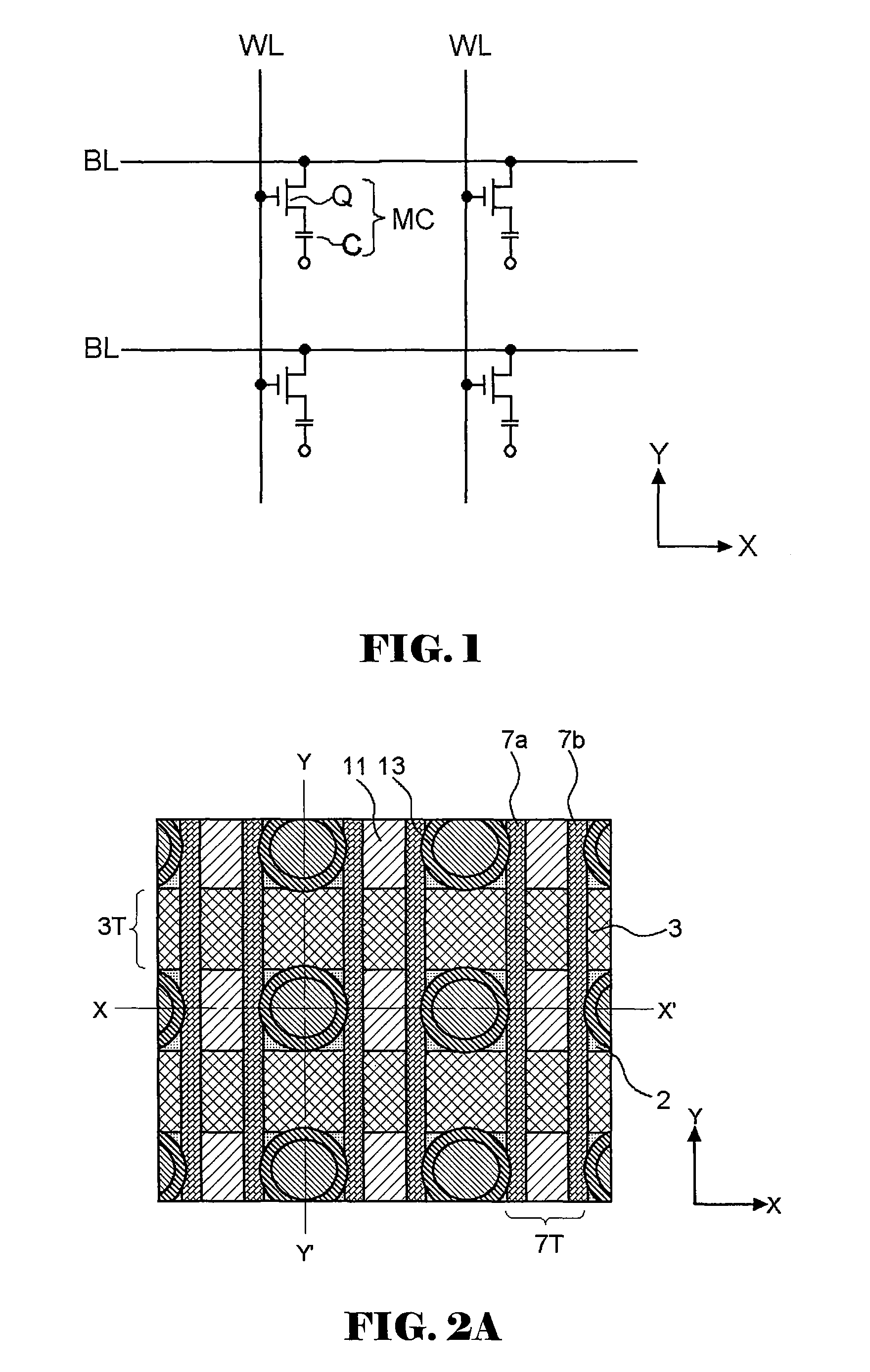
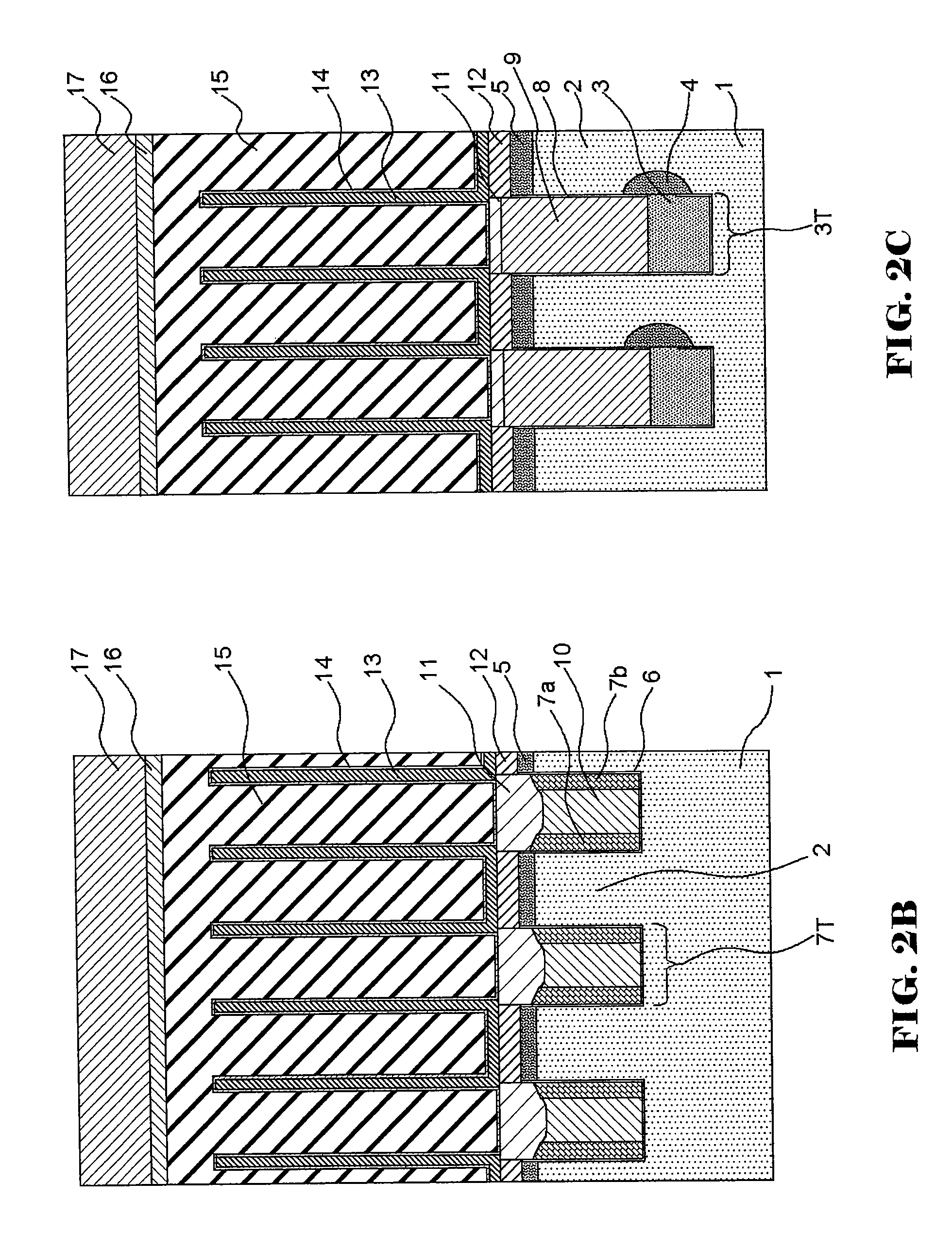
[0060]FIG. 3A to FIG. 12A and FIG. 14A to FIG. 17A are plan views; FIG. 3B to FIG. 12B, FIG. 14B to FIG. 17B, FIG. 18 and FIG. 19 are sectional views taken along a line X-X′; FIG. 3C to FIG. 12C and FIG. 14C to FIG. 17C are sectional views taken along a line Y-Y′; and FIG. 7D to FIG. 12D and FIG. 14D to FIG. 17D are sectional views taken along a line X1-X1′. These figures show a process of manufacturing a semiconductor device according to a first exemplary embodiment. Herein, an example will be described in which the invention is applied to a process of forming word lines 7a, 7b in trenches 7T for word line formation shown in FIG. 2A, FIG. 2B and FIG. 2C.

[0061]As shown in FIGS. 3A, 3B and 3C, mask nitride film 21 having a thickness of about 30 nm is formed on p-type silicon substrate 1.

[0062]Photoresist mask 22 is formed on mask nitride film 21 with ...

exemplary embodiment 2

[0119]In the followings, a process of manufacturing a semiconductor device according to a second exemplary embodiment will be described.

[0120]FIGS. 20 to 31 show processes of manufacturing a semiconductor device according to a second exemplary embodiment. FIGS. 20 to 31 are sectional views corresponding to the Y-Y′ sections in FIG. 2A.

[0121]Herein, an example will be described in which the invention is applied to a process of forming openings w29 connecting bit lines 3 and N-type impurity diffusion layers 4 formed in silicon pillars 2, which are shown in FIGS. 2A to 2C.

[0122]After forming trenches 3T for bit line formation as shown in FIG. 3, insulating film 8, which covers the sidewalls of silicon fins 2′ and bottom surfaces of trenches for bit line formation and is made of a silicon oxide film, is formed, as shown in FIG. 20. A conductive material film is formed so as to the trenches for bit line formation. The material of the film is a phosphorous-doped silicon film, for example....


PUM


Abstract

Disclosed is a method of manufacturing a semiconductor device comprising: forming a first layer on a sidewall of a trench formed on a main surface of a semiconductor substrate, filling up the trench with a protective film, etching back the protective film by a dry etching method so that a height of a surface of the protective film is lower than an opening of the trench and removing the first layer exposed by the etching-back.

Description

BACKGROUND OF THE INVENTION[0001]1. Field of the Invention[0002]The present invention relates to a method of manufacturing a semiconductor device, and more particularly, to a method of setting a surface height of a film, which is filled in a trench provided to a semiconductor substrate, to a position of a desired depth from an opening of the trench.[0003]2. Description of the Related Art[0004]The development of a high-integrated semiconductor device has been recently accelerated. As one of the approaches, it has been examined to adopt a vertical MOS transistor. For example, JP-A No. 2008-4915 (Patent Document 1) discloses a technology in which first and second source / drain areas are formed in upper and lower portions of a fin formed by a trench provided on a surface of a silicon substrate and a conductive material layer is provided to side faces of the trench via a dielectric layer, thereby forming a gate electrode. According to the technology, it is possible to reduce an area occup...

Claims


Application Information

Patent Timeline
Patent Type & Authority Patents(United States)
IPC IPC(8): H01L21/336
CPCH01L21/76232H01L27/10876H01L27/10891H01L29/66666H01L29/7827H10B12/053H10B12/488
Inventor OHTSUKA, KEISUKE
Owner LONGITUDE LICENSING LTD
Why Eureka
Try Eureka