Semiconductor package and method of manufacturing the same

a technology of semiconductors and components, applied in the direction of lighting and heating apparatus, electrical apparatus casings/cabinets/drawers, instruments, etc., can solve the problems of poor thermal performance, high thermal resistance, and substantial affecting the efficiency and reliability of components or modules

Active Publication Date: 2012-08-21
HONG KONG APPLIED SCI & TECH RES INST
View PDF48 Cites 15 Cited by
  • Summary
  • Abstract
  • Description
  • Claims
  • Application Information

AI Technical Summary

Benefits of technology

[0031]There are many advantages provided by the embodiments according to the present invention. First, the thermal resistance in the structure of the semiconductor package is substantially reduced and desirable performance of heat spreading or dissipation is achieved. Furthermore, since the structure can be easily realized by matured wafer-level or panel-level process on different kinds of substrate, the production cost of the package may also be reduced. Moreover, wafer-based lithography techniques are introduced in the present invention; therefore, the size of the LED module can be reduced as well.

Problems solved by technology

In a typical optoelectronic component or module, the issue concerning thermal spreading substantially affects the efficiency and reliability of the component or module.
As known in the art, high thermal resistance in the structure of the component or module results in poor thermal performance.
Usually, the problem concerning high thermal resistance was caused by materials or interfaces formed in the structure of the component or module.
However, satisfying heat spreading performance cannot be achieved merely by the conductive interconnect pattern LED and flexible substrate disclosed in this patent.
Since there is still a heat spreading barrier (the soft thermal conductive pad or paste) between LED and thermal conducting elements, satisfying performance of heat spreading is not achieved.
Obviously, there are too many layers stacked between LED and the thermal conduction element so that too many heat barriers are created in the structure.
However, as shown in the drawings and illustrated in the specification, the thermal element contacts merely the electrode such that the contacting area for spreading or dissipating heat is restricted.
Therefore, desired heat spreading performance cannot be obtained.
In addition, the discrete heat column / thermal via design only guides heat from the heat source to specific direction, which is insufficient for heat spreading.

Method used


Image

  • Semiconductor package and method of manufacturing the same
  • Semiconductor package and method of manufacturing the same
  • Semiconductor package and method of manufacturing the same

Examples


Embodiment Construction

.”

BRIEF DESCRIPTION OF THE DRAWING

[0015]Features, aspects, and embodiments are described in conjunction with the attached drawings, in which:

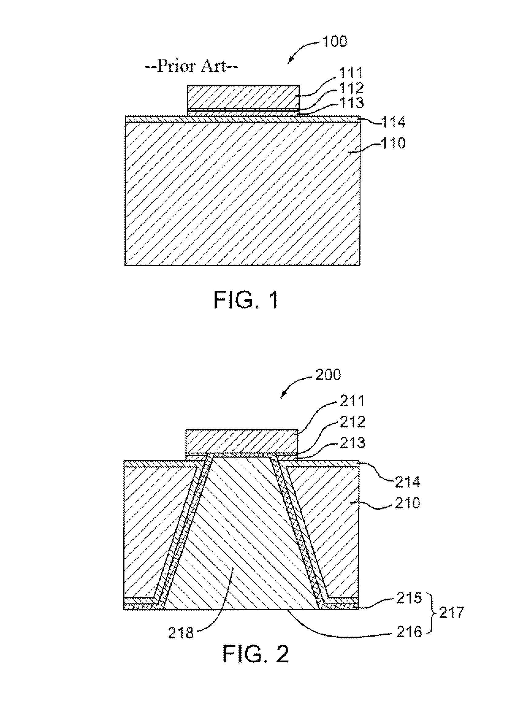
[0016]FIG. 1 is a side cross-sectional view illustrating the structure of a conventional package for an optoelectronic device.

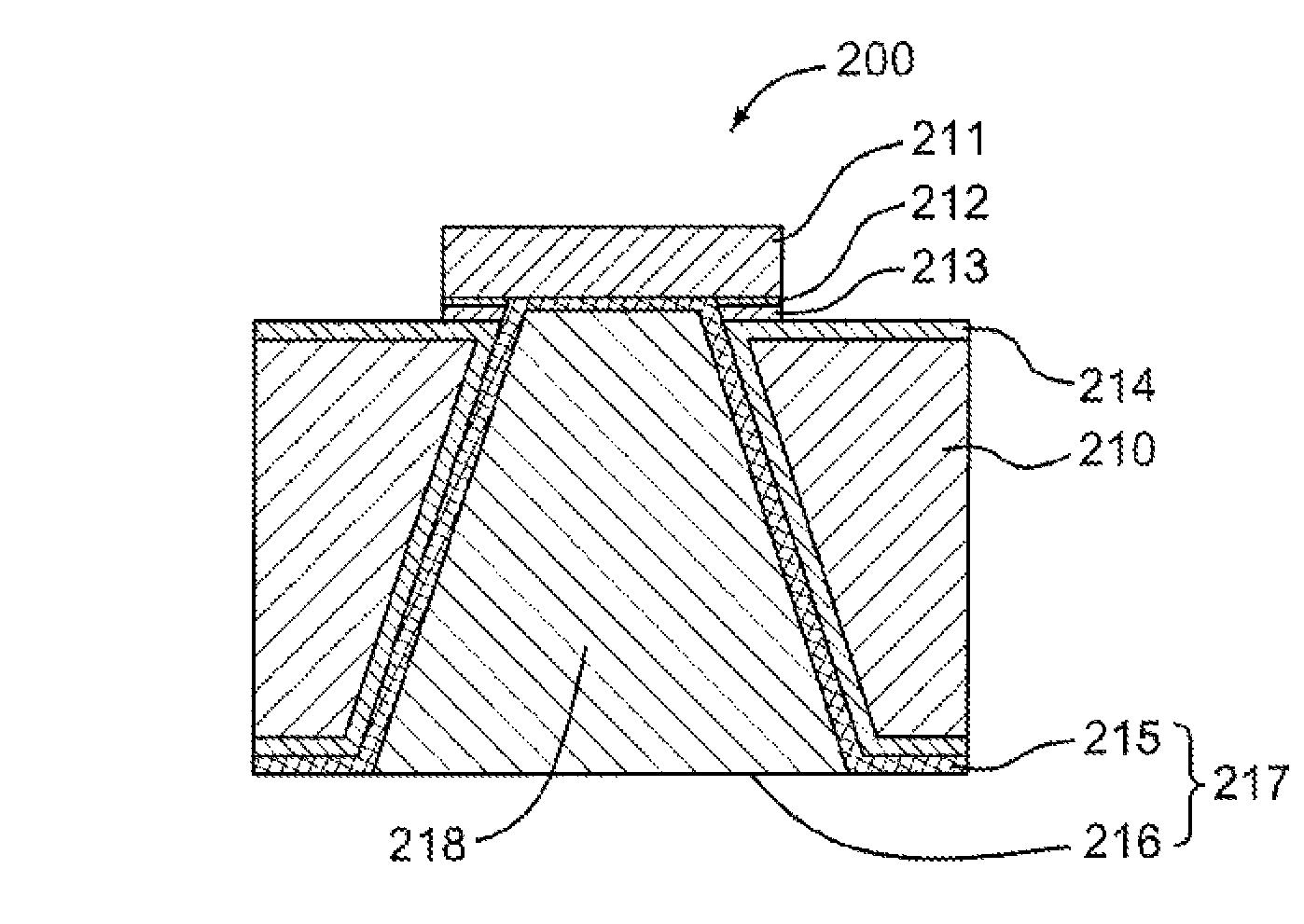
[0017]FIG. 2 is a side cross-sectional view illustrating the structure of the semiconductor package in accordance with the embodiment of the present invention.

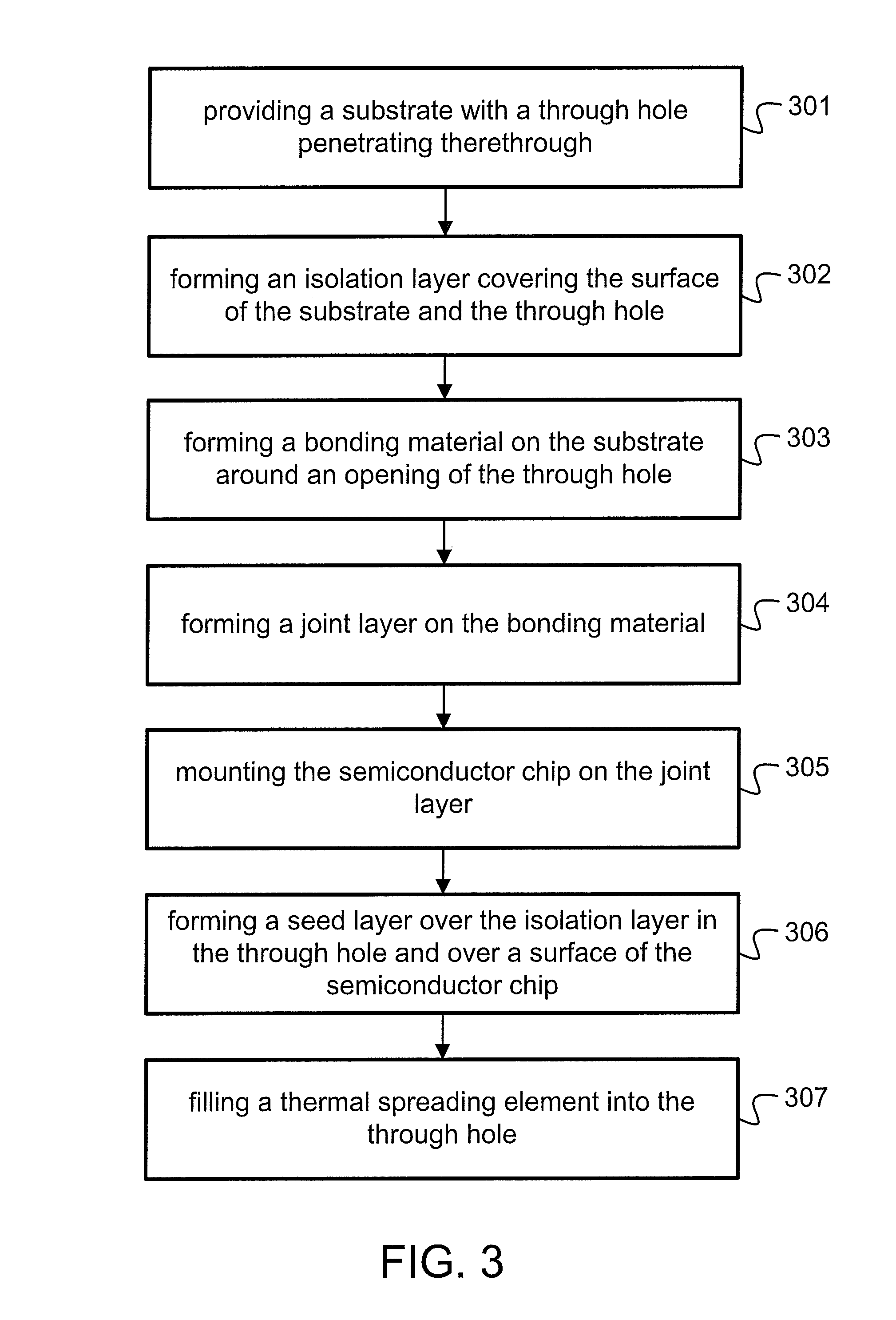
[0018]FIG. 3 shows a flowchart of manufacturing the semiconductor package according to the embodiment of the present invention.

[0019]FIG. 4A and FIG. 4B are diagrams showing the temperature distribution near the optoelectronic device in a conventional package and in the semiconductor package according to the present invention, respectively.

[0020]FIG. 5 is a line chart showing the relations between temperature and the distance from the central line of the semiconductor chip in the conventional package and in the semiconductor package according to the present inventi...


PUM


Abstract

The subject invention relates to a semiconductor package and method of manufacturing the same. The semiconductor package of the subject invention comprises a substrate with a through hole penetrating therethrough; a semiconductor chip positioned on the substrate covering the through hole; and a thermal conductive device filling the through hole and contacting the semiconductor chip. According to the subject invention, the thermal resistance in the structure of the semiconductor package is substantially reduced and thus desirable performance of heat spreading or dissipation is achieved. In addition, the production cost and size of the semiconductor package are also reduced.

Description

FIELD OF THE INVENTION[0001]The invention relates generally to a semiconductor package and, more particularly, to an optoelectronic semiconductor package having a heat spreading structure.BACKGROUND OF THE INVENTION[0002]In a typical optoelectronic component or module, the issue concerning thermal spreading substantially affects the efficiency and reliability of the component or module. As known in the art, high thermal resistance in the structure of the component or module results in poor thermal performance. Usually, the problem concerning high thermal resistance was caused by materials or interfaces formed in the structure of the component or module.[0003]FIG. 1 is a side cross-sectional view illustrating the structure of a conventional optoelectronic semiconductor package 100, which comprises a substrate 110, an optoelectronic semiconductor chip 111, a joint layer 112, a bonding metal 113, and an isolation layer 114. The conventional semiconductor package 100 is manufactured by ...

Claims


Application Information

Patent Timeline
Patent Type & Authority Patents(United States)
IPC IPC(8): H05K7/20
CPCH01L23/3677H01L33/642H01L33/641H01L2924/0002H01L2924/12044H01L2924/00
Inventor LIN, JYH-RONGLU, MING
Owner HONG KONG APPLIED SCI & TECH RES INST
Why Eureka
Try Eureka