Stacked photoelectric conversion device and method for producing the same

a photoelectric conversion and stacked technology, applied in the direction of semiconductor/solid-state device manufacturing, semiconductor devices, electrical devices, etc., can solve the problems of lack of raw materials in bulk solar cells, reduce the non-bonding hands of silicon, reduce the recombination of carriers, and enhance the photoelectric conversion efficiency

Inactive Publication Date: 2012-09-04
SHARP KK
View PDF12 Cites 13 Cited by
  • Summary
  • Abstract
  • Description
  • Claims
  • Application Information

AI Technical Summary

Benefits of technology

[0016]According to the present invention, there is provided a stacked photoelectric conversion device comprising a plurality of silicon-based photoelectric conversion layers having a p-i-n structure stacked, wherein at least a pair of adjacent photoelectric conversion layers have an interlayer of a silicon nitride therebetween, the pair of the photoelectric conversion layers are electrically connected with each other, and a p-type silicon-based semiconductor layer constituting a part of the photoelectric conversion layer and contacting the interlayer contains a nitrogen atom.
[0017]According to the present invention, the p-type silicon-based semiconductor layer contacting the interlayer of a silicon nitride contains a nitrogen atom, and the interlayer and the p-type silicon-based semiconductor layer are formed of materials of the same kind, thereby reducing non-bonding hands of silicon generated in the vicinity of an interface between the layers. Therefore, it is possible to decrease the carrier recombination and enhance the photoelectric conversion efficiency.
[0018]Additionally, in accordance with the present invention, when the interlayer has an aperture, it is possible to adjust the amount of reflected light to a cell (top cell) located at a light entrance side of the interlayer and the amount of incident light to a cell (bottom cell) located at a side opposite to the light entrance side of the interlayer by adjusting the size or the area density of the aperture. Therefore, the aperture can be formed so that the short circuit current density of the top cell and that of the bottom cell are equal, and therefore it is possible to obtain a stacked photoelectric conversion device of high efficiency.
[0020]The interlayer may have an aperture, and the pair of the photoelectric conversion layers may be electrically connected by contacting with, each other via the aperture. In this case, it is possible to electrically connect the pair of the photoelectric conversion layers each other more securely.
[0021]The p-type silicon-based semiconductor layer may contain nitrogen atoms of 0.001 to 10 atomic %. In this case, the effect of decreasing non-bonding hands of silicon is relatively significant (see Table 2).
[0022]The interlayer may contain nitrogen atoms of 10 to 60 atomic %. In this case, the difference in the index of refraction between the interlayer and the silicon-based photoelectric conversion layer is relatively large to allow the reflectance at the interface to be relatively large, and the area in which the interlayer is formed can be therefore relatively narrow (see Tables 3 and 4).

Problems solved by technology

Fossil fuels such as petroleum raise concerns about future depletion and have a problem of carbon dioxide emission causing global warming.
Recently, however, the bulk solar cells have had problems of lack of raw materials due to rapid increase of production volume and difficult cost reduction.

Method used


Image

  • Stacked photoelectric conversion device and method for producing the same
  • Stacked photoelectric conversion device and method for producing the same
  • Stacked photoelectric conversion device and method for producing the same

Examples


embodiment 1

1. Embodiment 1

Super-Strate Structure

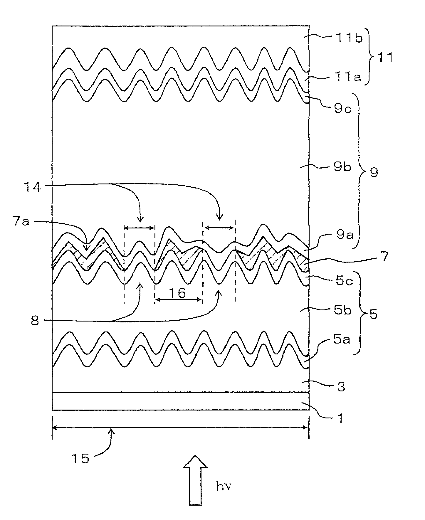
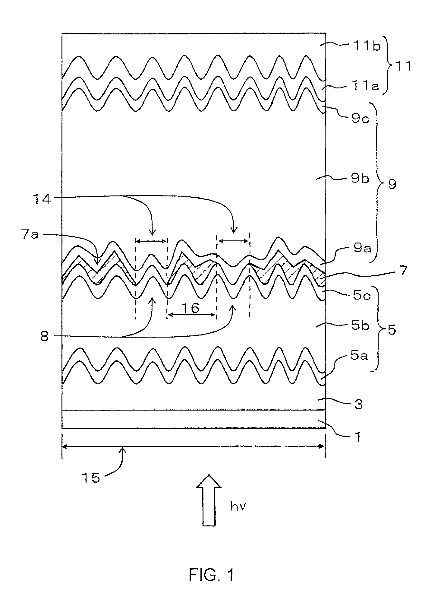
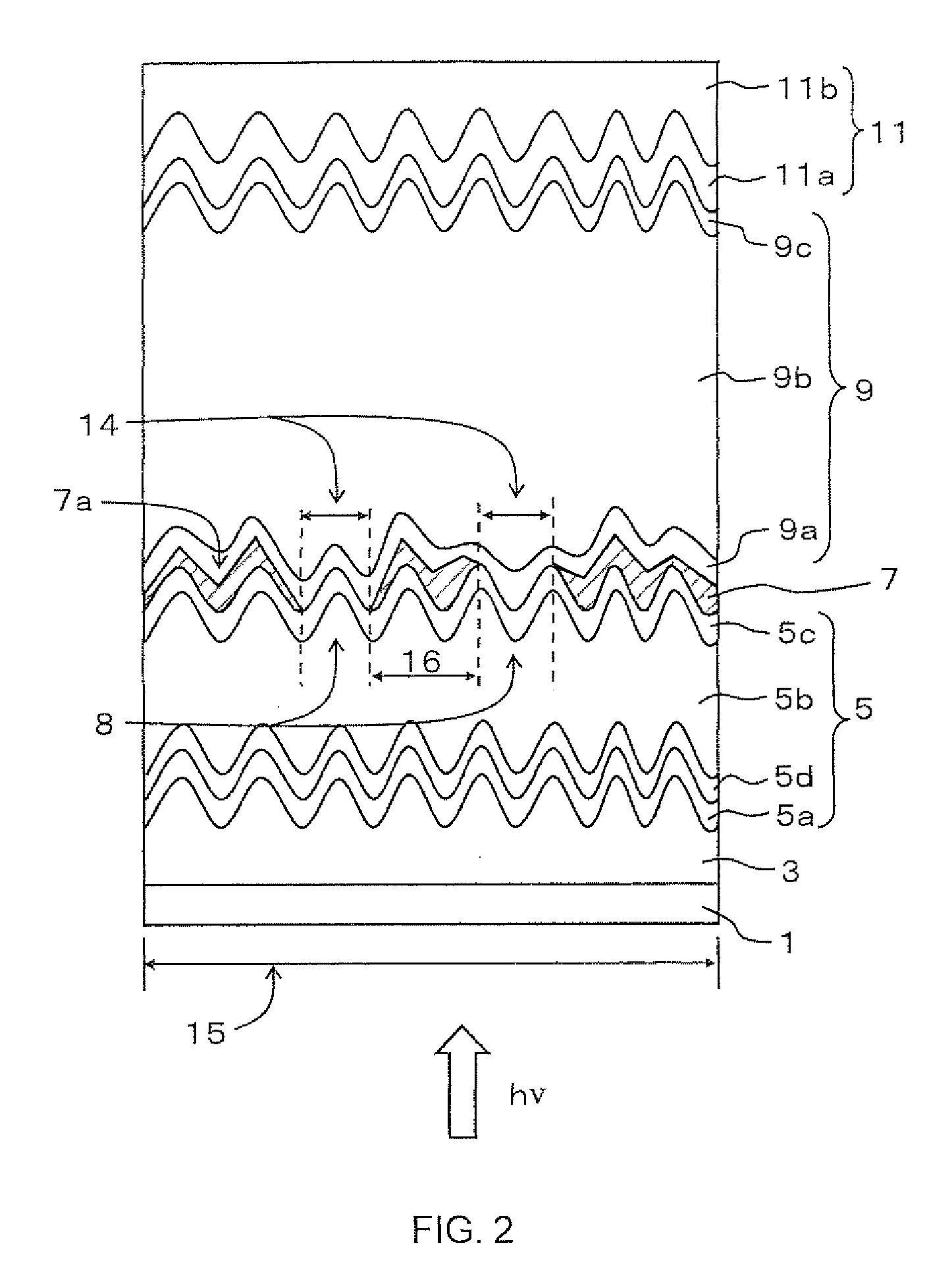
[0047]A photoelectric conversion device according to Embodiment 1 of the present invention comprises: a front transparent conductive layer, a plurality of silicon-based photoelectric conversion layers having a p-i-n structure, and a back electrode layer stacked in this order on a transparent substrate, wherein at least a pair of adjacent photoelectric conversion layers have an interlayer of a silicon nitride therebetween, the interlayer has at least one aperture, and the pair of photoelectric conversion layers (referred to as a first photoelectric conversion layer and a second photoelectric conversion layer from a side of the transparent substrate, respectively) having the interlayer therebetween contact with each other via the aperture, and a p-type silicon-based semiconductor layer constituting a part of the photoelectric conversion layer and contacting the interlayer contains a nitrogen atom.

[0048]When attention is paid to the pair of silicon ...

embodiment 2

2. Embodiment 2

Substrate Structure

[0095]A photoelectric conversion device according to Embodiment 2 of the present invention comprises: a plurality of silicon-based photoelectric conversion layers having a p-i-n structure, a transparent conductive layer, and a grid electrode stacked in this order on a metal substrate or a substrate having a surface coated with a metal, wherein at least a pair of adjacent photoelectric conversion layers have an interlayer of a silicon nitride therebetween, the interlayer has at least one aperture, and the pair of the photoelectric conversion layers (referred to as a first photoelectric conversion layer and a second photoelectric conversion layer from a side of the substrate, respectively) having the interlayer therebetween contact with each other via the aperture.

[0096]When attention is paid to the pair of silicon-based photoelectric conversion layers having the interlayer therebetween and having the p-i-n structure, in addition, the photoelectric co...

examples

[0107]Hereinafter, examples of the present invention will be described.

[0108]In the present examples, a stacked photoelectric conversion device of a superstraight type, comprising a photoelectric conversion layer having a hydrogenated amorphous silicon / a photoelectric conversion layer having a hydrogenated microcrystalline silicon will be described, for example.


PUM


Abstract

To provide a stacked photoelectric conversion device and a method for producing the same, in which an interlayer is provided between photoelectric conversion layers to obtain an effect of controlling the amount of incidence light, and carrier recombination at an interface between the interlayer and a semiconductor layer is decreased to enhance photoelectric conversion efficiency.The stacked photoelectric conversion device of the present invention comprises a plurality of silicon-based photoelectric conversion layers having a p-i-n structure stacked, wherein at least a pair of adjacent photoelectric conversion layers have an interlayer of a silicon nitride therebetween, the pair of the photoelectric conversion layers are electrically connected with each other, and a p-type silicon-based semiconductor layer constituting a part of the photoelectric conversion layer and contacting the interlayer contains a nitrogen atom.

Description

[0001]This application is the U.S. national phase of International Application No. PCT / JP2007 / 072207 filed 15 Nov. 2007, which designated the U.S. and claims priority to Japan Application No. 2007-012851 filed 23 Jan. 2007, the entire contents of each of which are hereby incorporated by reference.TECHNICAL FIELD[0002]The present invention at least in part relates to a stacked photoelectric conversion device and a method for producing the same. More particularly, the present invention relates to a stacked photoelectric conversion device having an interlayer between photoelectric conversion layers and a method for producing the same.BACKGROUND ART[0003]Fossil fuels such as petroleum raise concerns about future depletion and have a problem of carbon dioxide emission causing global warming. In recent years, spread of photovoltaic power systems has been expanded, and they are expected as an energy source alternative to fossil fuels such as petroleum because of increased environmental awa...

Claims


Application Information

Patent Timeline
Patent Type & Authority Patents(United States)
IPC IPC(8): H01L31/103H01L21/329
CPCH01L31/0236H01L31/076H01L31/022425Y02E10/548H01L31/02366
Inventor NASUNO, YOSHIYUKIKOHAMA, NORIYOSHINAKANO, TAKANORI
Owner SHARP KK
Why Eureka
Try Eureka