

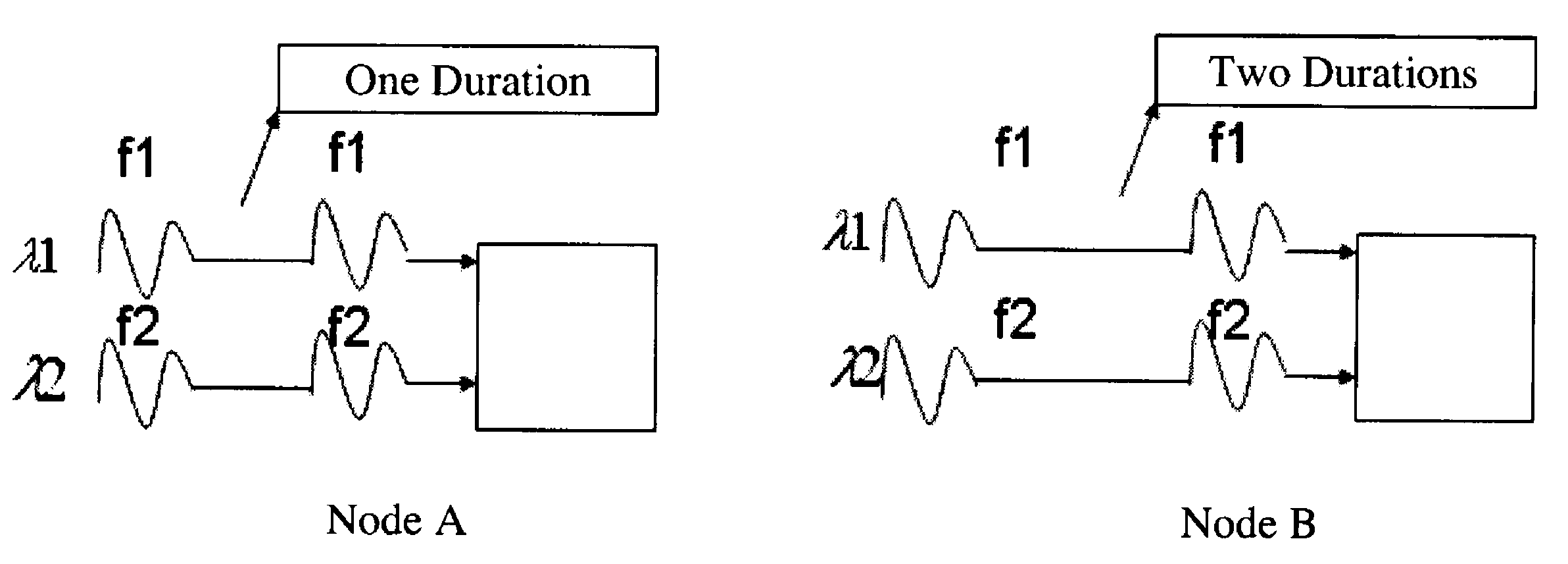
Light mark, method and device for light mark modulation and demodulation
a light mark and modulation technology, applied in the field of communication technology, can solve the problems of difficult identification of optical fiber connection relation, limited available frequency marks, and insufficient large-scale network, so as to reduce interference between marks with different wavelengths and power consumption of mark modulation devices.
- Summary
- Abstract
- Description
- Claims
- Application Information
AI Technical Summary
Benefits of technology
Problems solved by technology
Method used
Image

Examples
first embodiment
[0062]FIG. 7 is a schematic structural view of a device for light mark modulation according to the present disclosure. Referring to FIG. 7, the device includes a processor 70, a Direct Digital Synthesizer (DDS) 71, a switch 72, an amplifier 73, and a light modulator 74.
[0063]The processor is adapted to control the DDS 71 to generate a frequency mark, and control an amplification level of the frequency mark, so as to make the frequency mark meet the requirement.
[0064]The DDS 71 is connected to the processor 70, and controlled by the processor 70 to generate a corresponding frequency mark.
[0065]The switch 72 is connected to the processor 70 and the DDS 71, and controlled by the processor 70 to be turned on or off, so as to generate a mark with periodically alternating frequency and interval.
[0066]The amplifier 73, connected to the switch 72 and the processor 70, is adapted to receive the mark with periodically alternating frequency and interval, and controlled by the processor 70 to a...
second embodiment
[0074]FIG. 8 is a flow chart of a method for light mark modulation according to the present disclosure. Referring to FIG. 8, the method includes the following steps.
[0075]In Step 1, a DDS is controlled to generate a mark with periodically alternating frequency and interval.
[0076]The mark with periodically alternating frequency and interval may be generated by the DDS 71 under the control of a processor 70. Specifically, the processor 70 controls the DDS 71 to generate continuous frequency marks, and the processor 70 controls the frequency and the interval to appear in a periodically alternating manner by controlling the open or closed state of a circuit; or the processor controls the DDS 71 to directly generate the mark with periodically alternating frequency and interval.
[0077]In Step 2, the frequency mark with periodically alternating frequency and interval is amplified.
[0078]In Step 3, the frequency mark signal obtained after amplification is modulated onto an optical signal.
[007...
third embodiment
[0084]FIG. 9 is a schematic view of a device for light mark demodulation according to the present disclosure. Referring to FIG. 9, the device includes a signal receiving circuit and a digital processor 94.
[0085]The signal receiving circuit is adapted to split off a small portion of light from an optical signal modulated with a frequency mark, which is subjected to photoelectric conversion and analogue-to-digital conversion and then provided to the digital processor. The signal receiving circuit further includes a splitter 90, a photoelectric conversion unit 91, an amplifying and filtering unit 92, and an analogue-to-digital conversion unit 93.
[0086]The splitter 90 is adapted to split off a small portion of light from the optical signal modulated with the frequency mark.
[0087]The photoelectric conversion unit 91 is connected to the splitter 90, and adapted to receive the split light and photoelectrically convert the optical signal into an electrical signal.
[0088]The amplifying and fi...
PUM
 Abstract
Description
Claims
Application Information