Solid-state image sensor and imaging device

a solid-state image sensor and imaging device technology, applied in the field of solid-state image sensors and imaging devices, can solve the problems of increasing delay time, difficult to obtain appropriate trigger signals, increasing the size and weight of the system, etc., and achieve the effect of quick and reduced system costs

Active Publication Date: 2012-09-18
TOHOKU UNIV +1
View PDF18 Cites 8 Cited by
  • Summary
  • Abstract
  • Description
  • Claims
  • Application Information

AI Technical Summary

Benefits of technology

[0037]By the solid-state image sensor and imaging device according to the present invention, it is possible to quickly, i.e. with no significant delay in time, generate a trigger signal that correctly captures an occurrence of an objective phenomenon or a movement of or change in an object, so that the images of the objective phenomenon can be assuredly taken. Generating the trigger signal requires neither the detection signal of another sensor (e.g. a vibration sensor) nor an image taken with another imaging device. The trigger signal can be generated by the solid-state image sensor itself without using complex optical systems. Thus, the present technique is advantageous to reducing the system cost.

Problems solved by technology

However, in some situations, it is often difficult to obtain appropriate trigger signals by this method, as in the case where the sensor cannot be easily placed close to the object, where the imaging action must capture a spontaneous change in the object under observation, or where the imaging object is a micro-sized object under a microscope.
However, in the case of detecting a movement of or change in an object in real-time by image processing of the signals read from the image sensor, it is normally necessary to preserve the images in an external frame memory and perform a large amount of computation, which tends to increase the delay time from an occurrence of an objective phenomenon to the generation of a trigger signal.
Particularly, in the case of high-speed imaging, this delay time may prevent the objective phenomenon from being captured in the resultant images.
Thus, the system will be large and complex, making it difficult to reduce the production cost and decrease the size and weight of the system.
However, providing the change detection element within the image sensor area inevitably lowers the quality of the resultant images since the pixel signals required for the imaging cannot be obtained at the portion where the change detection element is present.
However, as in the conventional technique described in Patent Document 2, using an optical system for light-splitting purposes significantly increases the production cost.
Furthermore, detecting a change that occurs within a portion of the imaging range requires a considerable number of change detection elements, which increases the chip area of the solid-state image sensor and accordingly increases the production cost.

Method used


Image

  • Solid-state image sensor and imaging device
  • Solid-state image sensor and imaging device
  • Solid-state image sensor and imaging device

Examples


Embodiment Construction

[0063]A solid-state image sensor and an imaging device which is an embodiment of the present invention is hereinafter described with reference to the attached drawings.

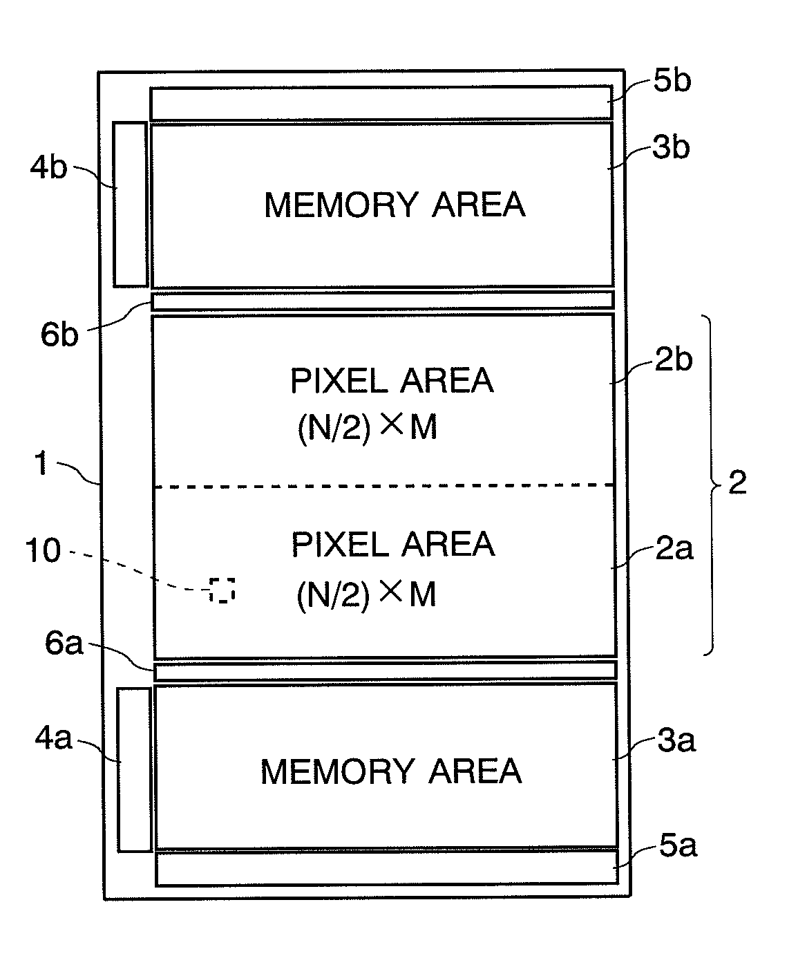
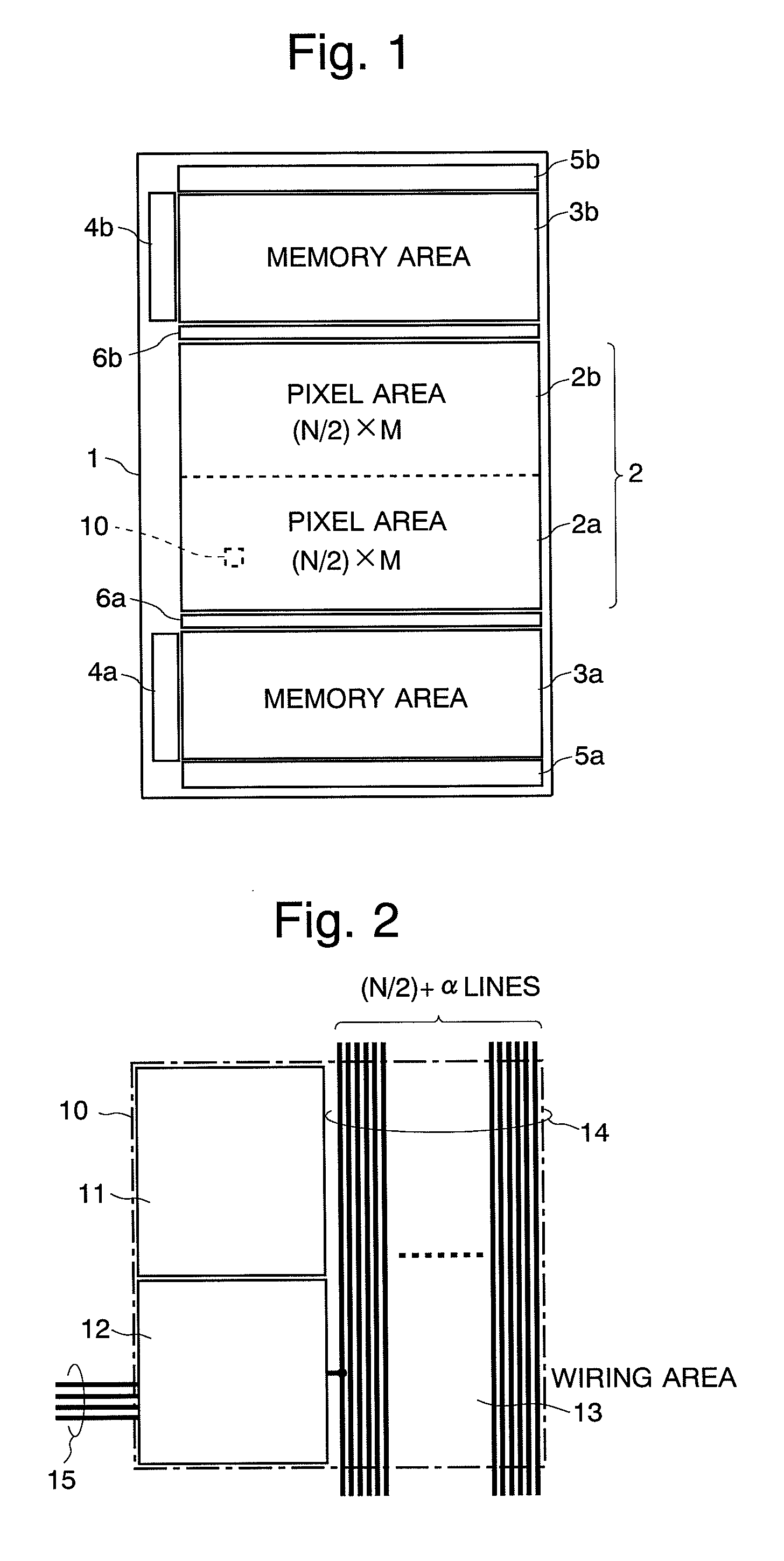
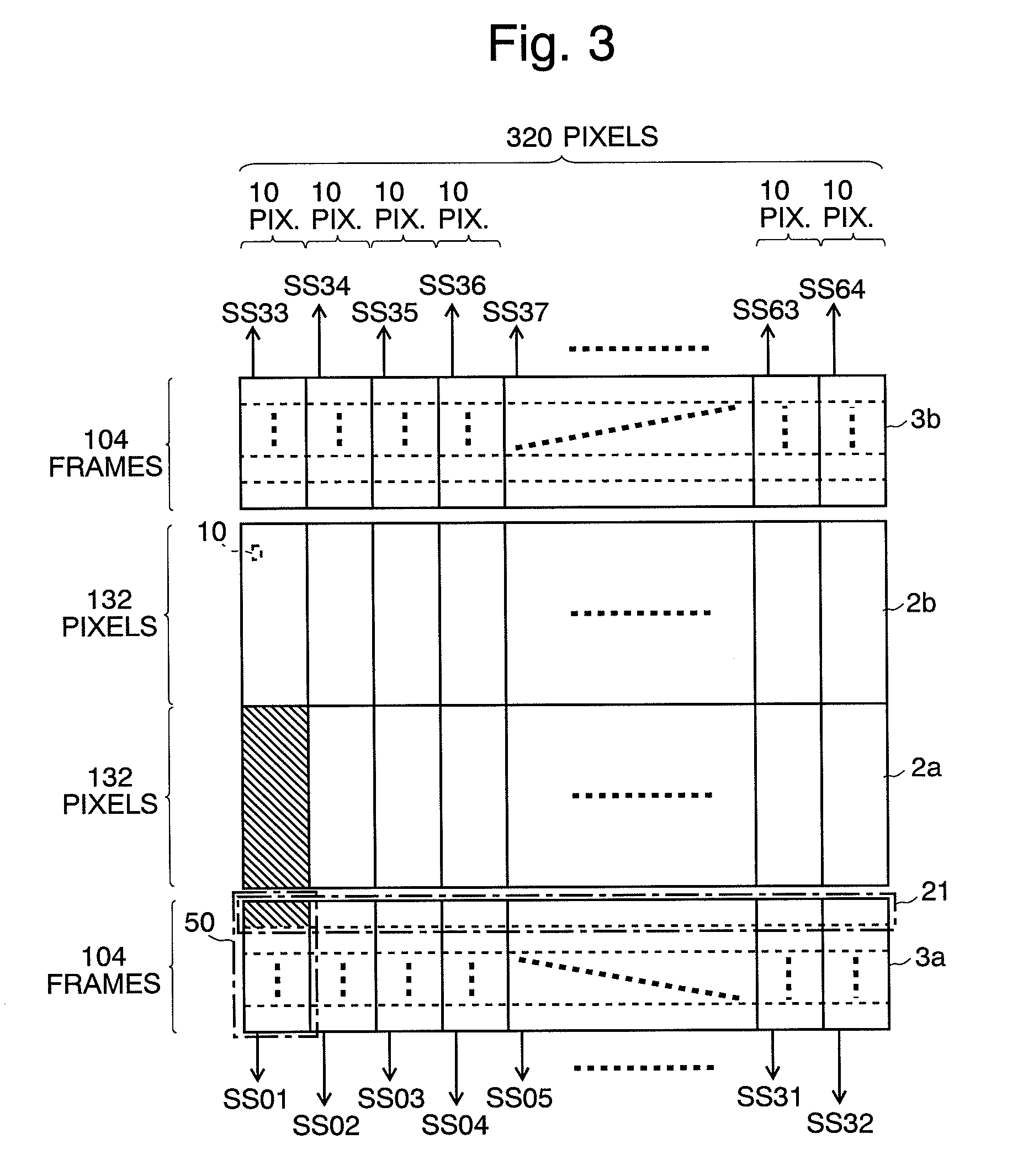
[0064]An overall configuration and structure of the solid-state image sensor according to the present embodiment is initially described. FIG. 1 is a schematic plan view showing the layout on a semiconductor chip of the solid-state image sensor of the present embodiment, FIG. 3 is a plan view showing a schematic configuration of the pixel area and memory area in the solid-state image sensor of the present embodiment, and FIG. 4 is a block diagram of the main portion corresponding to approximately one-half of the semiconductor chip of the solid-state image sensor of the present embodiment.

[0065]As shown in FIG. 1, in the present solid-state image sensor, the pixel area 2 (2a and 2b) for receiving light and producing signals for each pixel and the memory areas 3a and 3b for holding the signals for a predetermined number ...


PUM


Abstract

A pixel output line (14) is independently provided for each of the pixels arranged in a two-dimensionally array within a pixel area so that pixel signals can be sequentially written in a plurality of memory sections (22) through the pixel output lines (14). When a plurality of frames of pixel signals are held in the memory sections (22), the pixel signals corresponding to two arbitrarily selected frames are read and respectively stored in sample-and-hold circuits (61 and 62), and their difference is obtained. Then, the difference signals corresponding to a predetermined range of the image are integrated, and the integrated value is compared with a threshold. If the integrated value exceeds the threshold, it is presumed that a change in an imaging object has occurred, and a pulse generation circuit (66) generates a trigger signal. By controlling the discontinuation and other imaging actions according to this trigger signal, it is possible to correctly take high-speed images of the situation before or after the occurrence of an objective phenomenon.

Description

CROSS REFERENCE TO RELATED APPLICATIONS[0001]This application is a National Stage of International Application No. PCT / JP2008 / 002427 filed Sep. 4, 2008, claiming priority based on Japanese Patent Application No. 2007-230180, filed Sep. 5, 2007, the contents of all of which are incorporated herein by reference in their entirety.TECHNICAL FIELD[0002]The present invention relates to a solid-state image sensor and an imaging device using the solid-state image sensor. More specifically, it relates to a solid-state image sensor and imaging device capable of high-speed operations suitable for taking images of high-speed phenomena, such as destructions, explosions and combustions, and a drive method for such a sensor.BACKGROUND ART[0003]High-speed imaging devices (high-speed video cameras) for taking consecutive images of high-speed phenomena such as explosions, destructions, combustions, collisions and discharges for only a short period of time have been conventionally developed (for examp...

Claims


Application Information

Patent Timeline
Patent Type & Authority Patents(United States)
IPC IPC(8): H04N5/228H04N5/335H04N5/374
CPCH04N3/155H04N5/374H04N5/378H04N25/41H04N25/59H04N25/76H04N25/75
Inventor SUGAWA, SHIGETOSHIKONDO, YASUSHITOMINAGA, HIDEKI
Owner TOHOKU UNIV
Why Eureka
Try Eureka