Memory system

a memory system and memory technology, applied in the field of memory systems, can solve the problems of unnecessarily repeated rewriting, and achieve the effects of reducing system cost, improving effective life, and more reliable system

Active Publication Date: 2007-05-10
SONY CORP
View PDF8 Cites 148 Cited by
  • Summary
  • Abstract
  • Description
  • Claims
  • Application Information

AI Technical Summary

Benefits of technology

[0034] Preferably, it is possible to arbitrarily set the system selection for the Passive-wear-leveling control and the Active-wear-leveling control and the condition setting values of both the kinds of Wear-leveling.
[0035] According to the embodiments of the invention, it is possible to perform optimum Wear-leveling control even when data having the first data area in which data is frequently rewritten and the second data area in which data is hardly rewritten mixed therein is stored, and it is possible to substantially improve an effective life in terms of the number of times of rewriting by the memory system in which the nonvolatile semiconductor storage device is used.
[0036] Since the number of times of rewriting of the memory system is increased, it goes without saying that a more reliable system can be provided. Moreover, the extension of the life in terms of the number of times of rewriting leads to a reduction in cost of the system.

Problems solved by technology

As a result, rewriting may be performed a large number of times unnecessarily.

Method used


Image

  • Memory system
  • Memory system
  • Memory system

Examples


Embodiment Construction

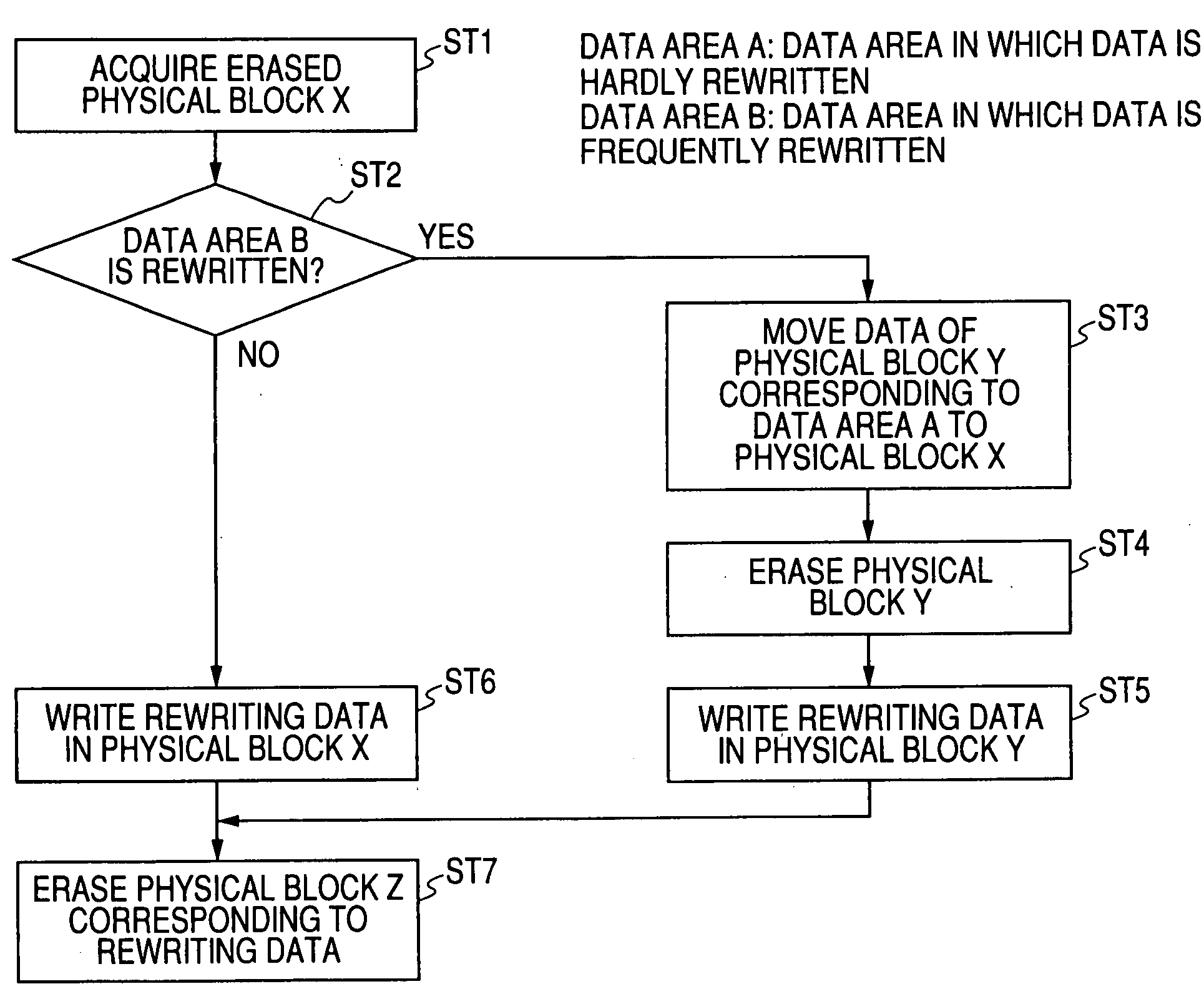
[0056] An embodiment of the invention will be hereinafter explained with reference to the drawings.

[0057]FIG. 5 is a diagram showing a memory system (a storage) according to the embodiment of the invention.

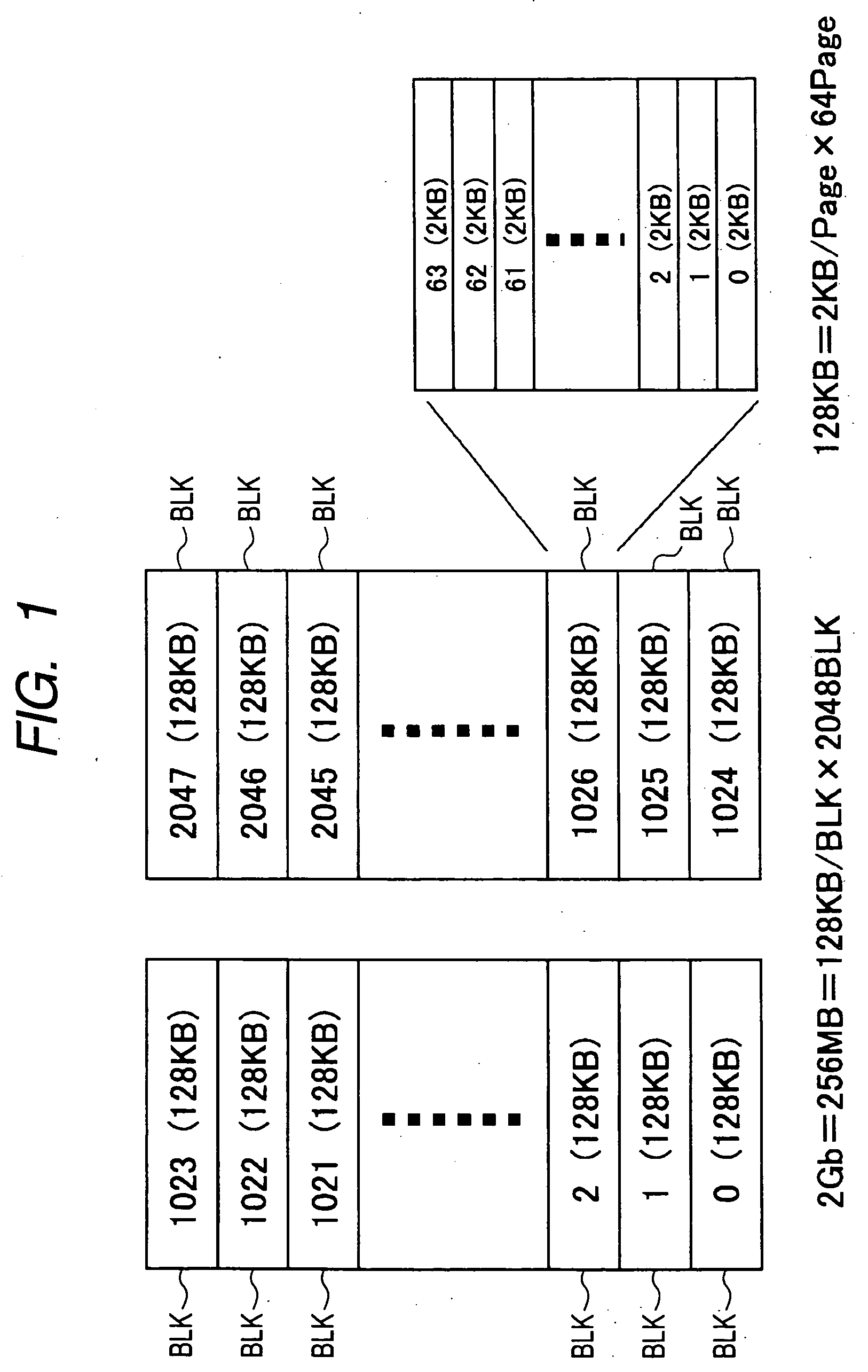
[0058] A memory system (a storage) 10 in FIG. 5 has, as main components, a NAND flash memory 11 serving as a nonvolatile memory unit, a page buffer 12, a control unit 13, an interface circuit (I / F) 14, and an internal data bus 15.

[0059] In the memory system 10, a one-chip NAND flash memory 11, which has, for example, a 16-bit input / output, is connected in parallel to the internal data bus 15.

[0060] The page buffer 12 temporarily stores, via the internal data bus 15, page data accessed. The page buffer 12 is connected to the interface circuit 14 with the outside.

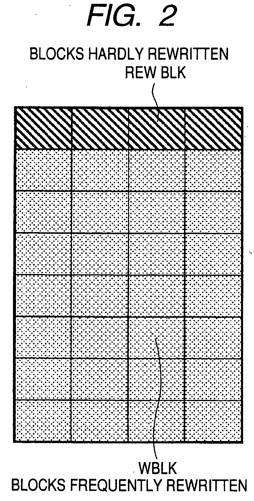
[0061] The control unit 13 performs control of access to the flash memory 11 on the basis of an improved Wear-leveling control system. As explained later, the control unit 13 typically realizes optimum Wear-leveling co...


PUM


Abstract

A memory system including a nonvolatile semiconductor storage device includes: a nonvolatile memory unit that includes a first data area in which data is frequently rewritten and a second data area in which data is hardly rewritten; and a control unit. The control unit sequentially selects logical block addresses in the second data area in which data is hardly rewritten and updates physical block addresses at new rewriting destinations in the first data area in which data is frequently rewritten to physical block addresses corresponding to the logical block addresses selected.

Description

CROSS-REFERENCES TO RELATED APPLICATIONS [0001] This application contains subject matter related to Japanese Patent Application JP 2005-326414 filed in the Japanese Patent Office on Nov. 10, 2005, the entire contents of which being incorporated herein by reference. BACKGROUND OF THE INVENTION [0002] 1. Field of the Invention The present invention relates to a memory system including a nonvolatile semiconductor storage device, and, more particularly to a technique for improving a Wear-leveling control system in a memory system having a data area in which data is frequently rewritten and a data area hardly written mixed therein. [0003] 2. Description of the Related Art [0004] As one of semiconductor storage devices, a flash memory. that can be electrically written is known. Above all, a NAND flash memory in which plural memory cells are connected in series to constitute a NAND cell block attracts attention as a flash memory that can be highly integrated. [0005] One memory cell of the ...

Claims


Application Information

Patent Timeline
Patent Type & Authority Applications(United States)
IPC IPC(8): G11C16/04G06F12/00
CPCG06F12/0246G06F2212/1036G06F2212/7211G11C16/349G11C16/3495
Inventor SAKUI, KOJISUZUKI, KAZUHIROYOSHIOKA, DAISUKEKAMIMURA, KAZUTOISHIMOTO, TAKESHISUMINO, JUN
Owner SONY CORP
Why Eureka
Try Eureka