
Sub-word line driver circuit and semiconductor memory device having the same

a sub-word line driver and memory device technology, applied in the direction of oscillator generators, digital storage, instruments, etc., can solve the problem of serious delay in driving a selected word line connected to a relatively large number of memory cells, and achieve the effect of increasing the effective channel length of transistors

Active Publication Date: 2012-10-02
SAMSUNG ELECTRONICS CO LTD
View PDF13 Cites 4 Cited by
  • Summary
  • Abstract
  • Description
  • Claims
  • Application Information

AI Technical Summary

Benefits of technology

The patent text describes a sub-word line driver circuit and a semiconductor memory device including the circuit. The circuit and device can increase the effective channel length of transistors, which can improve performance. The circuit includes a substrate, gate lines, and a gate tab that covers an isolation area. The gate tab can be enlarged in the second direction to further cover a boundary portion of an active area. The memory device includes a sub-word line driver and a memory cell array, where each memory cell is connected to the sub-word line and a bit line. Overall, the technical effects of the patent text are improved performance and efficiency of the sub-word line driver circuit and semiconductor memory device.

Problems solved by technology

When the current-driving capacity of the word line driver is limited, a delay in driving a selected word line connected to a relatively large number of memory cells becomes serious.

Method used


Image

  • Sub-word line driver circuit and semiconductor memory device having the same
  • Sub-word line driver circuit and semiconductor memory device having the same
  • Sub-word line driver circuit and semiconductor memory device having the same

Examples


Embodiment Construction

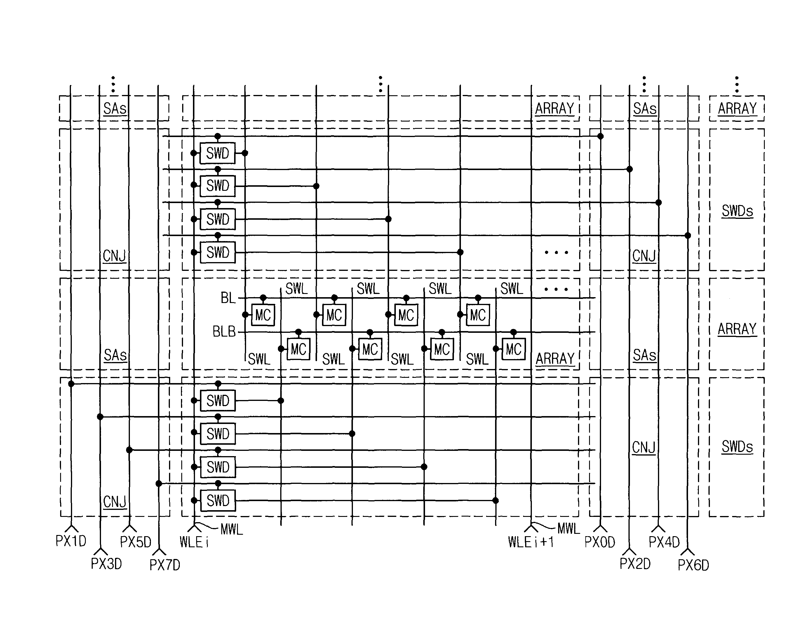
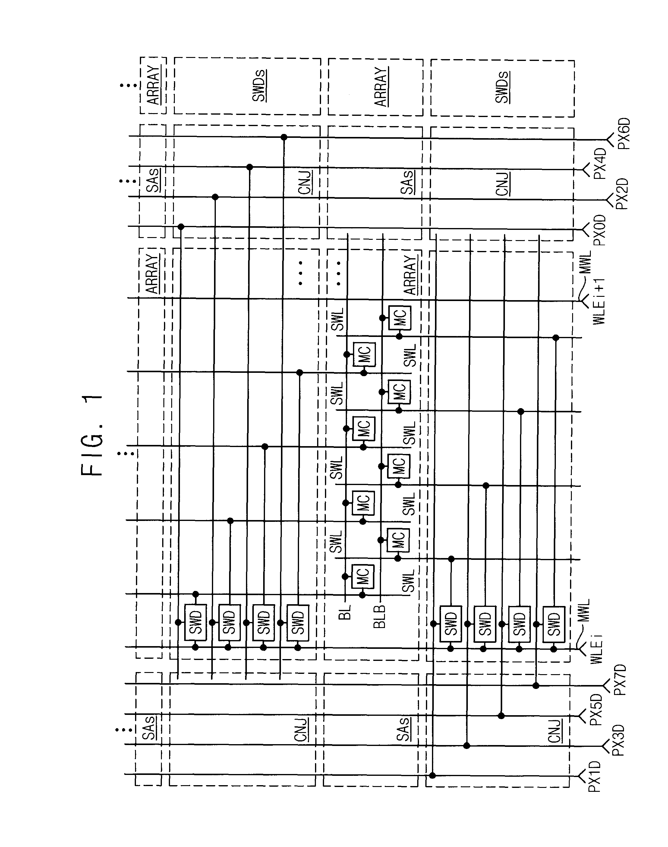
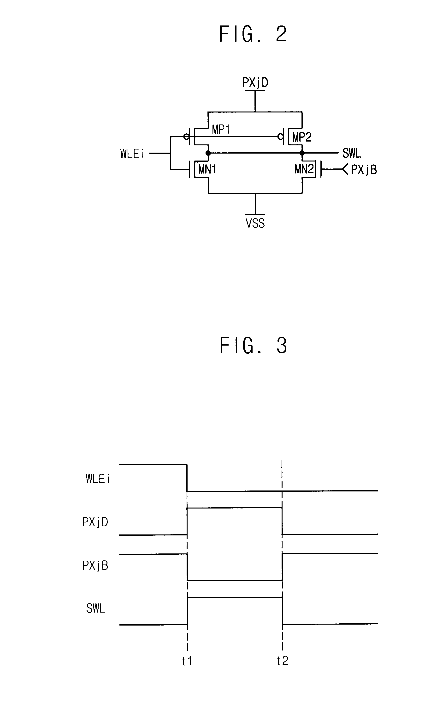
[0031]Various example embodiments will be described more fully hereinafter with reference to the accompanying drawings, in which some example embodiments are shown. The present inventive concept may, however, be embodied in many different forms and should not be construed as limited to the example embodiments set forth herein. Rather, these example embodiments are provided so that this disclosure will be thorough and complete, and will fully convey the scope of the present inventive concept to those skilled in the art. In the drawings, the sizes and relative sizes of layers and regions may be exaggerated for clarity. Like numerals refer to like elements throughout.

[0032]It will be understood that, although the terms first, second, third etc. may be used herein to describe various elements, these elements should not be limited by these terms. These terms are used to distinguish one element from another. Thus, a first element discussed below could be termed a second element without de...


PUM


Abstract

A sub-word line driver includes a substrate, a plurality of gate lines and at least one gate tab. The substrate includes a plurality of isolation areas and a plurality of active areas, where the two active areas are separated by each isolation area, and the isolation areas and the active areas are extended in a first direction and are arranged in a second direction perpendicular to the first direction. The plurality of gate lines are formed on the substrate, where the gate lines are extended in a second direction and are arranged in the first direction. The at least one gate tab is formed on the substrate, where the at least one gate tab is extended in the first direction to cover the isolation area. Incorrect operation of the sub-word line driver may be prevented, and a power consumption of the sub-word line driver may be reduced.

Description

CROSS-REFERENCE TO RELATED APPLICATION(S)[0001]This application claims priority under 35 USC §119 to Korean Patent Application No. 2009-0073207, filed on Aug. 10, 2009, in the Korean Intellectual Property Office (KIPO), the contents of which are incorporated herein in its entirety by reference.BACKGROUND[0002]1. Technical Field[0003]Example embodiments relate to a semiconductor memory device, and more particularly to a layout of a sub-word line driver circuit and a semiconductor memory device having a sub-word line driver circuit.[0004]2. Description of the Related Art[0005]Semiconductor memory devices are configured to store data into and read data from memory cells connected to word lines and bit lines. Memory cells connected to one word line are selected simultaneously based on a word line voltage that is applied to the one word line.[0006]As storage capacity of a semiconductor memory device increases, more memory cells are connected to one word line and thus a current-driving ca...

Claims


Application Information

Patent Timeline
Patent Type & Authority Patents(United States)
IPC IPC(8): G11C8/00H01L29/76H01L21/70
CPCG11C8/08G11C5/02G11C5/06
Inventor YANG, HYANG-JAPARK, JEONG-SOO
Owner SAMSUNG ELECTRONICS CO LTD
Learn More