Solid-state memory device, data processing system, and data processing device
a memory device and data processing technology, applied in semiconductor devices, digital storage, instruments, etc., can solve problems such as inability to solve techniques, difficulty in greatly reducing the current required to change a phase, and large current, and achieve good reproducibility and good reproducibility. , the effect of very few fluctuations
- Summary
- Abstract
- Description
- Claims
- Application Information
AI Technical Summary
Benefits of technology
Problems solved by technology
Method used
Image

Examples
first embodiment
[0066]FIG. 3 is across-sectional view showing a configuration of the superlattice laminate SL according to the present invention.
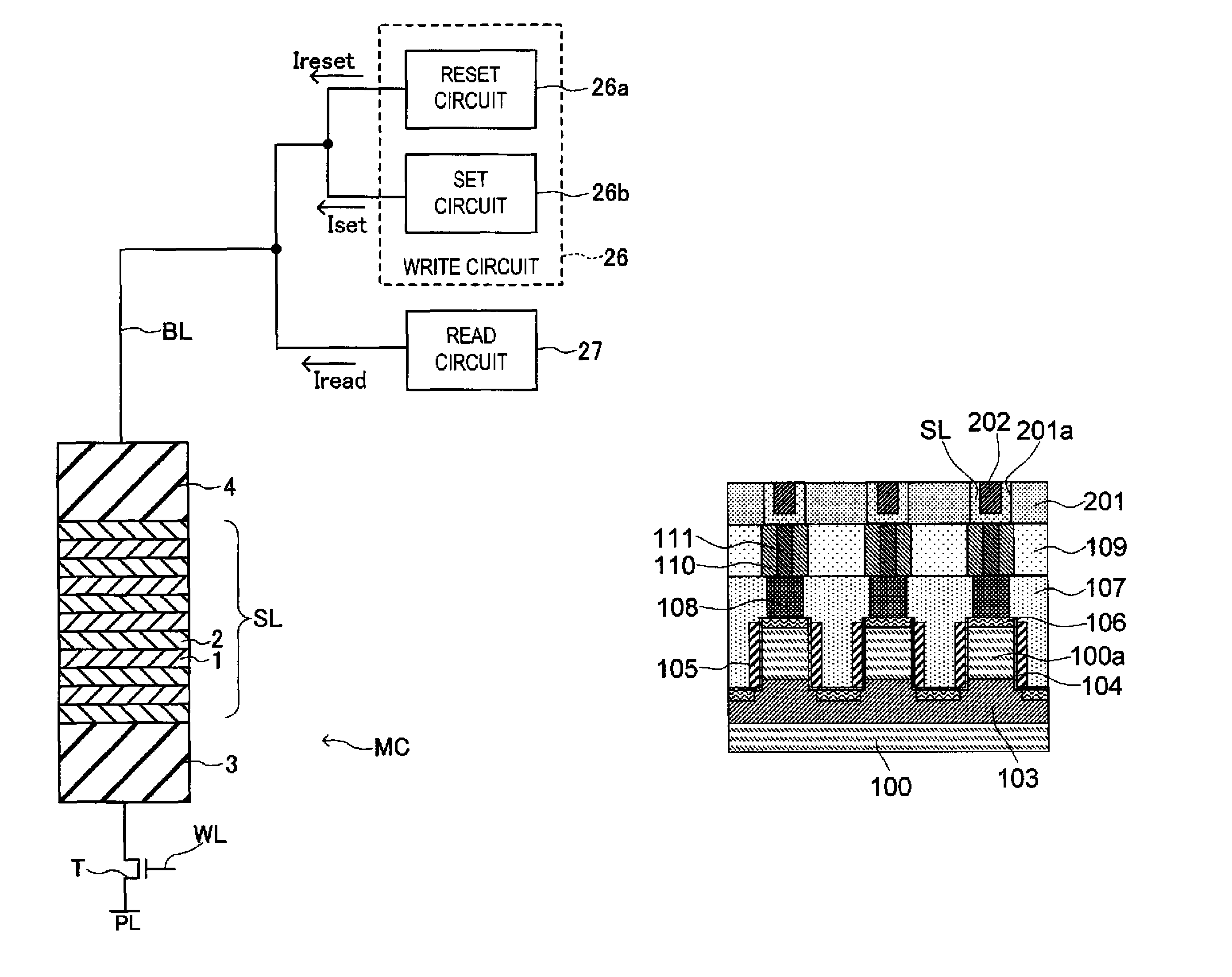
[0067]As shown in FIG. 3, the superlattice laminate SL used for a memory element according to the first embodiment has a crystal layer 1 and a crystal layer 2 laminated alternately in plural layers. A lower electrode 3 is provided on one surface SLa of the superlattice laminate SL in its laminating direction, and an upper electrode 4 is provided on the other surface SLb of the superlattice laminate SL in its laminating direction. That is, the superlattice laminate SL is sandwiched between these electrodes 3 and 4, and a laminating direction of the superlattice laminate SL coincides with opposite directions of the electrodes 3 and 4.
[0068]In this configuration, when a current is passed to the superlattice laminate SL via the electrodes 3 and 4, the current flows to a laminating direction of the superlattice laminate SL. Unlike bulk-shaped materials, the sup...
second embodiment
[0139]A configuration of the memory cells MC according to the present invention is explained next.
[0140]FIGS. 20A to 20C show a device configuration of the memory cells MC according to the second embodiment, where FIG. 20A is a schematic cross-sectional view along a bit line direction (a Y direction), FIG. 20B is a schematic cross-sectional view along a word line direction (an X direction), and FIG. 20C is an enlarged schematic cross-sectional view of a region C shown in FIG. 20A.
[0141]The memory cells MC shown in FIGS. 20A and 20B are different from the memory cells MC (according to the first embodiment) shown in FIGS. 7A and 7B, in a configuration of an upper part from the interlayer insulation film 109. Other features of the memory cells MC according to the second embodiment are identical to those of the first embodiment, and thus like elements are denoted by like reference numerals and redundant explanations thereof will be omitted.
[0142]In the second embodiment, interlayer insu...
third embodiment
[0148]A configuration of the memory cells MC according to the present invention is explained next.
[0149]FIGS. 23A to 23C show a device configuration of the memory cells MC according to the third embodiment, where FIG. 23A is a schematic cross-sectional view along a bit line direction (the Y direction), FIG. 23B is a schematic cross-sectional view along a word line direction (the X direction), and FIG. 23C is an enlarged schematic cross-sectional view of a region C shown in FIG. 23A.
[0150]The memory cells MC shown in FIGS. 23A and 23B are different from the memory cells MC (according to the second embodiment) shown in FIGS. 20A and 20B, in a configuration of an upper part from the interlayer insulation films 201. Other features of the memory cells MC according to the third embodiment are identical to those of the second embodiment, and thus like elements are denoted by like reference numerals and redundant explanations thereof will be omitted.
[0151]In the third embodiment, upper surf...
PUM
 Abstract
Description
Claims
Application Information
 - R&D Engineer
- R&D Manager
- IP Professional
- Industry Leading Data Capabilities
- Powerful AI technology
- Patent DNA Extraction
Browse by: Latest US Patents, China's latest patents, Technical Efficacy Thesaurus, Application Domain, Technology Topic.
© 2024 PatSnap. All rights reserved.Legal|Privacy policy|Modern Slavery Act Transparency Statement|Sitemap