Test structure for charged particle beam inspection and method for defect determination using the same

a charge particle and beam inspection technology, applied in the field of test structures, can solve problems such as difficult inspection of sub-threshold leakage within static random access memory arrays, difficult identification of defective mosfets with sub-threshold leakage, and occurrence of sub-threshold leakag

Active Publication Date: 2012-10-30
ASML NETHERLANDS BV
View PDF16 Cites 62 Cited by
  • Summary
  • Abstract
  • Description
  • Claims
  • Application Information

AI Technical Summary

Problems solved by technology

Other causes such as a changed threshold voltage value of a device transistor due to wrongly implanted dopant type or non-uniform dopant distribution would also lead to the occurrence of sub-threshold leakage.
However, the sub-threshold leakage within a static random access memory (SRAM) array is not easy to be inspected by charged particle beam inspection such as EBI, because the scanning charged particle beam gives rise to an equal surface charging (thus surface potential) to plugs with a similar underneath connected electrical devices.
This makes it difficult to identify the defective MOSFET which has sub-threshold leakages.

Method used


Image

  • Test structure for charged particle beam inspection and method for defect determination using the same
  • Test structure for charged particle beam inspection and method for defect determination using the same
  • Test structure for charged particle beam inspection and method for defect determination using the same

Examples


Embodiment Construction

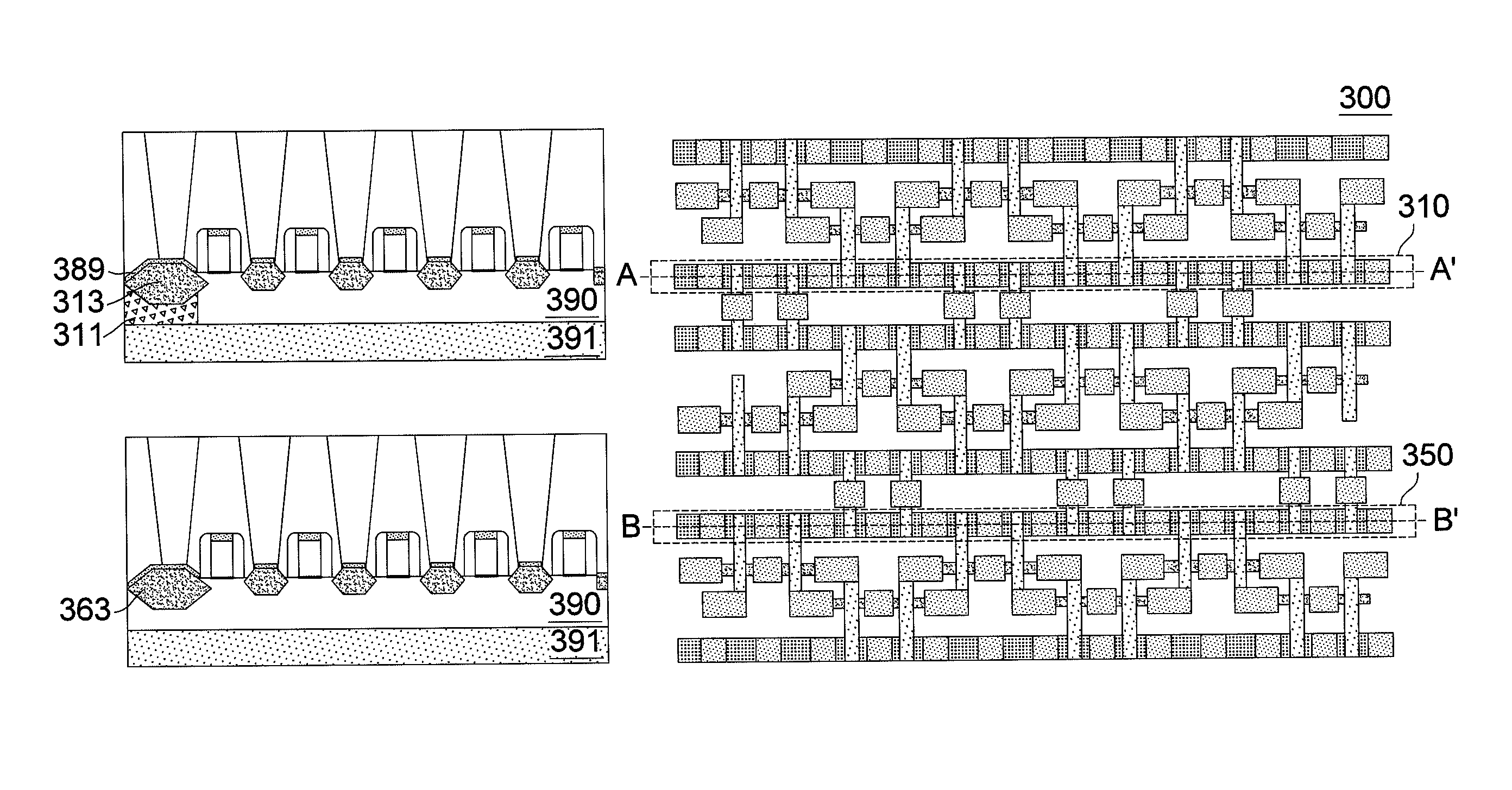
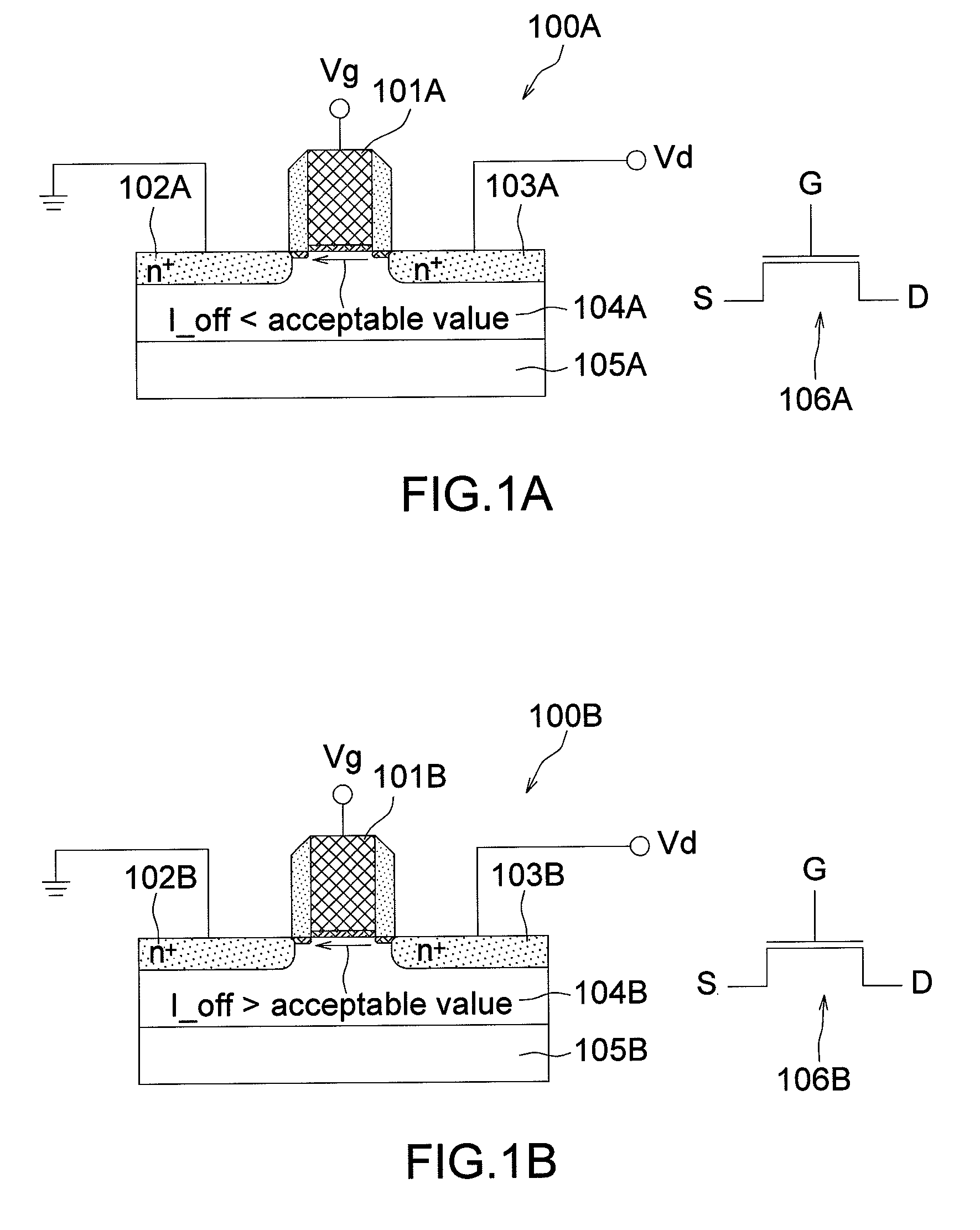
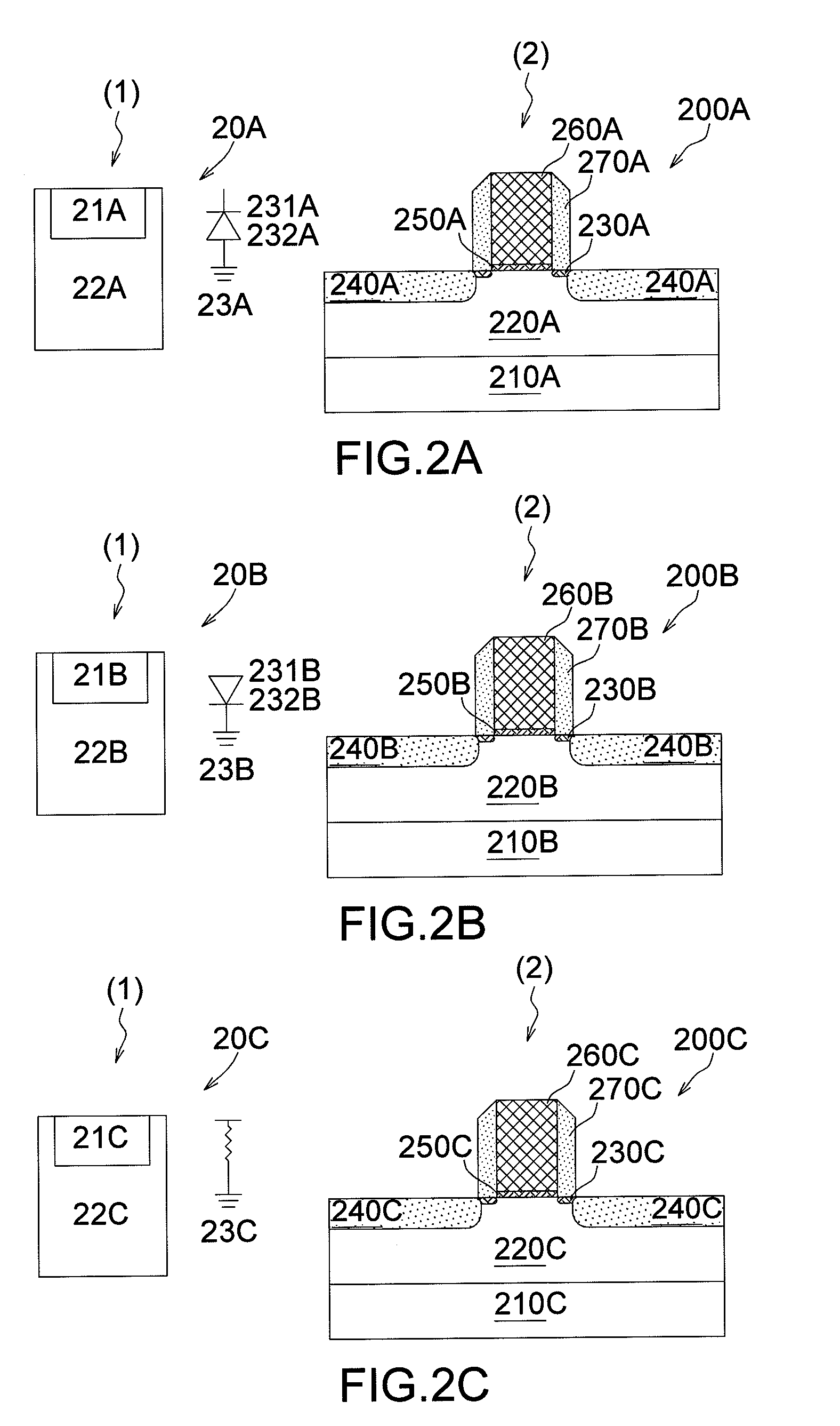
[0048]Various example embodiments of the present invention will now be described more fully with reference to the accompanying drawings in which some example embodiments of the invention are shown. In the drawings, the thicknesses of layers and regions may be exaggerated for clarity.

[0049]Detailed illustrative embodiments of the present invention are disclosed herein. However, specific structural and functional details disclosed herein are merely representative for purposes of describing example embodiments of the present invention. This invention may, however, may be embodied in many alternate forms and should not be construed as limited to only the embodiments set forth herein.

[0050]Accordingly, while example embodiments of the invention are capable of various modifications and alternative forms, embodiments thereof are shown by way of example in the drawings and will herein be described in detail. It should be understood, however, that there is no intent to limit example embodime...


PUM


Abstract

A test structure and method thereof for determining a defect in a sample of semiconductor device includes at least one transistor rendered grounded. The grounded transistor is preferably located at least one end of a test pattern designed to be included in the sample. When the test structure is inspected by charged particle beam inspection, the voltage contrast (VC) of the transistors in the test pattern including the grounded transistor is observed for determination of the presence of defect in the sample.

Description

CROSS REFERENCE TO RELATED APPLICATION[0001]This application is a Continuation-In-Part of Application No. 12 / 420,224, filed Apr. 8, 2009, the entire contents of which are herein meant to be incorporated by reference.BACKGROUND OF THE INVENTION[0002]1. Field of the Invention[0003]The present invention relates to a test structure and its application for inspecting an electrical device; and more particularly, relates to a test structure and method for detecting sub-threshold leakage defect in an electrical device.[0004]2. Description of the Prior Art[0005]The sub-threshold leakage is a current that flows from the drain to source of a metal-oxide-semiconductor-field-effect-transistor (MOSFET) when the transistor is supposed to be off. When the transistor is turned off or the voltage supplied to the gate of the transistor is lower than its threshold voltage, ideally the conduction between the drain and source should be smaller than a predefined acceptable value, wherein this value is mai...

Claims


Application Information

Patent Timeline
Patent Type & Authority Patents(United States)
IPC IPC(8): H01L23/58H01L23/62
CPCG01R31/307G01R31/2884H01L2924/0002H01L2924/00
Inventor XIAO, HONG
Owner ASML NETHERLANDS BV
Why Eureka
Try Eureka