Apparatus and methods for semiconductor IC failure detection

a technology of failure detection and apparatus, applied in the direction of semiconductor/solid-state device testing/measurement, instruments, electrical excitation analysis, etc., can solve the problems of two adjacent lines having the same potential, scanned portion is classified as defect, and produces a high potential during voltage contrast inspection

Inactive Publication Date: 2006-02-07
KLA TENCOR TECH CORP
View PDF25 Cites 77 Cited by
  • Summary
  • Abstract
  • Description
  • Claims
  • Application Information

AI Technical Summary

Benefits of technology

[0014]In another embodiment, the invention pertains to a method of inspecting a test structure. Two or more initial portions of the test structure are initially scanned with a charged particle beam to determine whether there is a defect present within the test structure based on whether there is an unexpected pattern of voltage potentials present within the test structure as a result of the initial scanning. When a defect is present, one or more potential defect portions of the test structure are sequentially stepped to, and the one or more potential defect portions of the test structure are scanned with a charged particle beam to thereby locate the defect.
[0015]In one implementation, the stepping is in the form of a binary search pattern for locating the defect. In another implementation, the operation of initially scanning two or more initial portions of the test structure with a charged particle beam to determine whether there is a defect present is accomplished by scanning a first end of the test structure to obtain a first potential for the first end, scanning a second end of the test structure to obtain a second potential for the second end, and determining that the test structure has an open defect when the first end potential differs from the second end potential.
[0016]In another aspect, the operation of stepping to one or more potential defect portions of the test structure and scanning the one or more potential defect portions of the test structure with a charged particle beam to thereby locate the defect includes a) stepping to a first current portion of the test structure and scanning the first current portion of the test structure for a defect, b) when the defect is not found and a transition in intensity occurs between the previous scan and current scan, stepping to a next portion of the test structure that is between the previous scan and the current scan, and c) when the defect is not found and a transition in intensity does not occur between the previo...

Problems solved by technology

Hence, when the scanned portion's potential and resulting image appearance differs significantly from the expected result, the scanned portion is classified a defect.
If there is an open defect present within a line that is supposedly coupled to ground, this open will cause a portion of the line to be left at a floating potential to thereby produce a high potential during the voltage contrast inspection.
Both open and short defects causes two adjacent lines to have a same potential during the voltage inspection.
Unfortunately, conventional voltage contrast test structures have associated disadvantages.
Another more significant deficiency of the conventional voltage contrast t...

Method used


Image

  • Apparatus and methods for semiconductor IC failure detection
  • Apparatus and methods for semiconductor IC failure detection
  • Apparatus and methods for semiconductor IC failure detection

Examples


Embodiment Construction

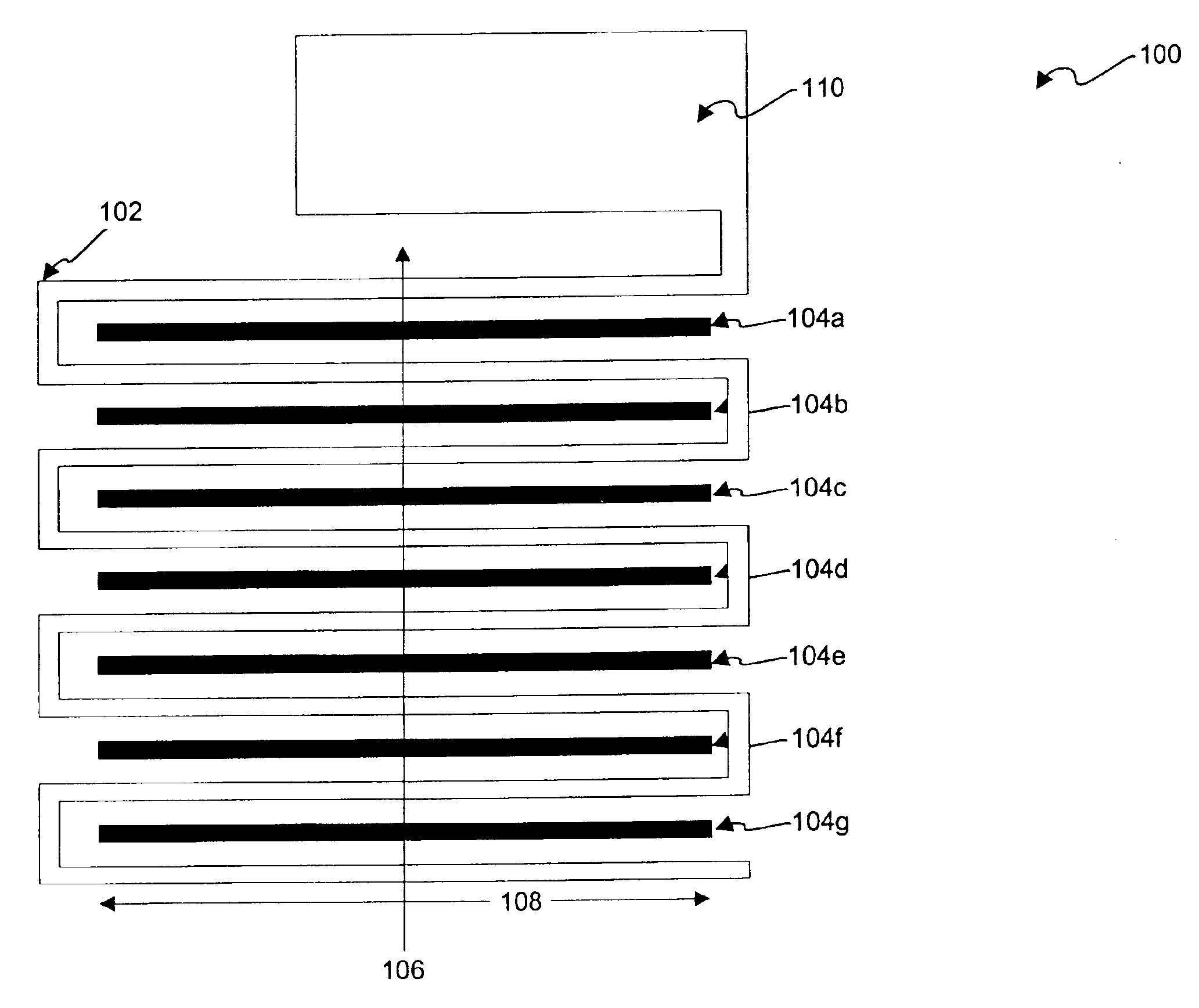
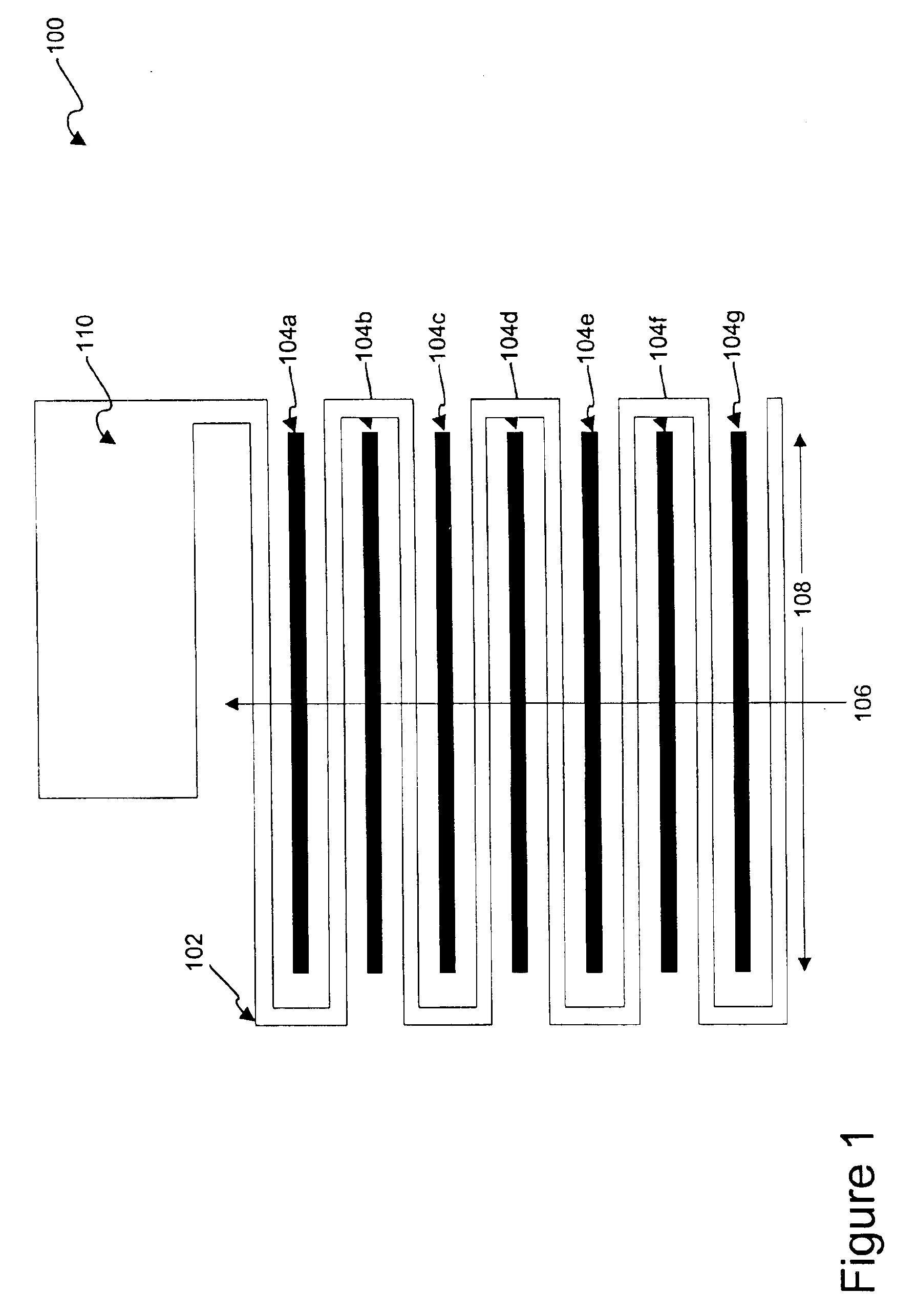
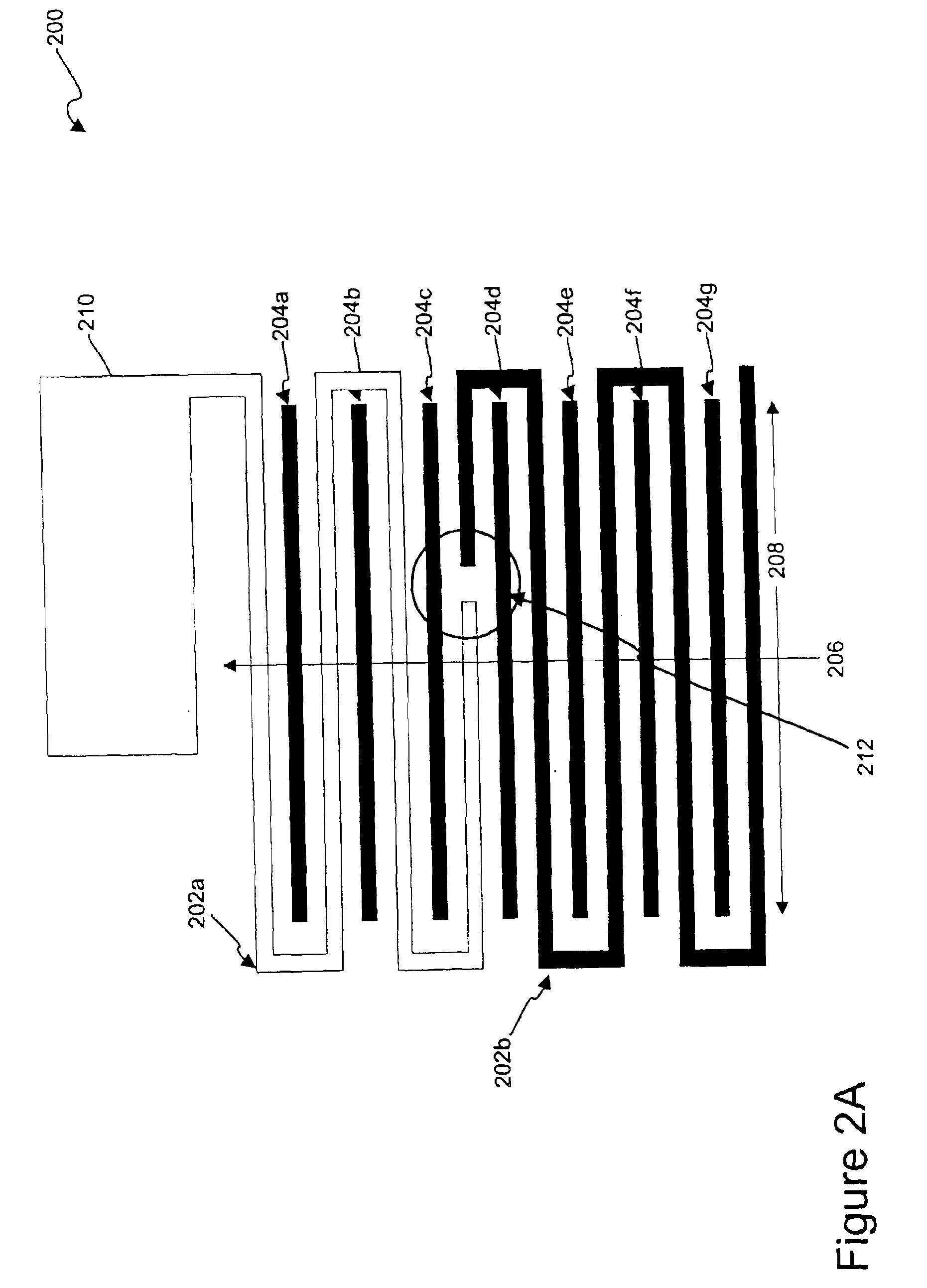
[0026]Reference will now be made in detail to a specific embodiment of the invention. An example of this embodiment is illustrated in the accompanying drawings. While the invention will be described in conjunction with this specific embodiment, it will be understood that it is not intended to limit the invention to one embodiment. On the contrary, it is intended to cover alternatives, modifications, and equivalents as may be included within the spirit and scope of the invention as defined by the appended claims. In the following description, numerous specific details are set forth in order to provide a thorough understanding of the present invention. The present invention may be practiced without some or all of these specific details. In other instances, well known process operations have not been described in detail in order not to unnecessarily obscure the present invention.

[0027]In general terms, one embodiment of the present invention provides voltage contrast based test structu...


PUM


Abstract

An improved voltage contrast test structure is disclosed. In general terms, the test structure can be fabricated in a single photolithography step or with a single reticle or mask. The test structure includes substructures which are designed to have a particular voltage potential pattern during a voltage contrast inspection. For example, when an electron beam is scanned across the test structure, an expected pattern of intensities are produced and imaged as a result of the expected voltage potentials of the test structure. However, when there is an unexpected pattern of voltage potentials present during the voltage contrast inspection, this indicates that a defect is present within the test structure. To produce different voltage potentials, a first set of substructures are coupled to a relatively large conductive structure, such as a large conductive pad, so that the first set of substructures charges more slowly than a second set of substructures that are not coupled to the relatively large conductive structure. Mechanisms for fabricating such a test structure are also disclosed. Additionally, searching mechanisms for quickly locating defects within such a test structure, as well as other types of voltage contrast structures, during a voltage contrast inspection are also provided.

Description

CROSS REFERENCE TO RELATED APPLICATIONS[0001]This application is a continuation-in-part and claims priority of U.S. patent application Ser. No. 09 / 648,380, entitled TEST STRUCTURES AND METHODS FOR INSPECTION OF SEMICONDUCTOR INTEGRATED CIRCUITS, filed 25 Aug. 2000 now U.S. Pat. No. 6,528,818, by Akella V.S. Satya et al., which application is incorporated herein by reference in its entirety for all purposes.[0002]This application also claims priority of the U.S. Provisional Application, having an application No. 60 / 329,804, entitled APPARATUS AND METHODS FOR SEMICONDUCTOR IC FAILURE DETECTION, filed 17 Oct. 2001, by Kurt H. Weiner et al., which application is incorporated herein by reference in its entirety for all purposes.BACKGROUND OF THE INVENTION[0003]This invention relates to methods and apparatus for detecting electrical defects in a semiconductor device or test structure having a plurality of features that are specifically designed to produce varying voltage potentials during...

Claims


Application Information

Patent Timeline
IPC IPC(8): H01L23/58G01N21/95G01R31/26G01R31/307H01L23/544
CPCG01N21/66G01N21/9501G01N21/956H01L22/34G01R31/307G01R31/2644G01R31/2884H01J2237/2817
Inventor WEINER, KURT H.VERMA, GAURAV
Owner KLA TENCOR TECH CORP
Why Eureka
Try Eureka