Methods for identifying an allowable process margin for integrated circuits

a technology of integrated circuits and process margins, which is applied in the direction of semiconductor/solid-state device testing/measurement, semiconductor/solid-state device details, instruments, etc., can solve the problems of inability to provide further information on detected defects, increasing circuit-packing densities of substrates, and increasing complexity of electronic circuits on substrates

Active Publication Date: 2010-01-05
SAMSUNG ELECTRONICS CO LTD
View PDF4 Cites 81 Cited by
  • Summary
  • Abstract
  • Description
  • Claims
  • Application Information

AI Technical Summary

Problems solved by technology

For this reason, electronic circuits on substrates are becoming more and more complicated, and circuit-packing densities for the substrates are gradually increasing.
However, there is a problem in that the TEG inspection technology cannot provide any further information on detected defects such as the kinds, locations and causes of the defects.
However, the above voltage contrast inspection technology provides accurate information on the processing defects generated in each of the unit processes of the manufacturing process for the semiconductor device, but typically does not provide any information on a process margin of each of the unit processes.
In general, the processing defects, which may reduce a production yield of a semiconductor device, are classified into random defects caused by particles or voids, and system defects caused by insufficient transcription of a layout for a circuit pattern.
Random defects represent all kinds of the processing defects that are randomly and unintentionally generated in the unit processes of the manufacturing process for the semiconductor device, and includes electrical or physical defects caused by random particles or random voids that are unintentionally generated in the manufacturing process.
When a circuit pattern is formed to have smaller critical dimensions (CD) using a usual apparatus for the unit process having conventional specifications and operational characteristics, the layout for the circuit pattern may be difficult to accurately transcribe onto a substrate, to thereby increase the possibility of system defects due to the poor accuracy of the transcription.
Accordingly, there may be a higher possibility of system defects being generated due to discrepancies between the circuit pattern on a substrate and the circuit layout.
The conventional defect inspection technology discussed above has been good for detecting random defects that have already been generated in a unit process; however, the conventional defect inspection technology generally cannot provide any information on system defects that may be generated after the unit process has been completed.
Furthermore, a recent manufacturing process has a higher chance of generating system defects due to high process accuracy that is required for patterns having reduced CDs and line widths.
In contrast, system defects are caused by incomplete transcription of the layout onto the substrate, and thus the inspection technology for system defects is focused on obtaining a sufficient allowable error range or process margin.

Method used


Image

  • Methods for identifying an allowable process margin for integrated circuits
  • Methods for identifying an allowable process margin for integrated circuits
  • Methods for identifying an allowable process margin for integrated circuits

Examples


Embodiment Construction

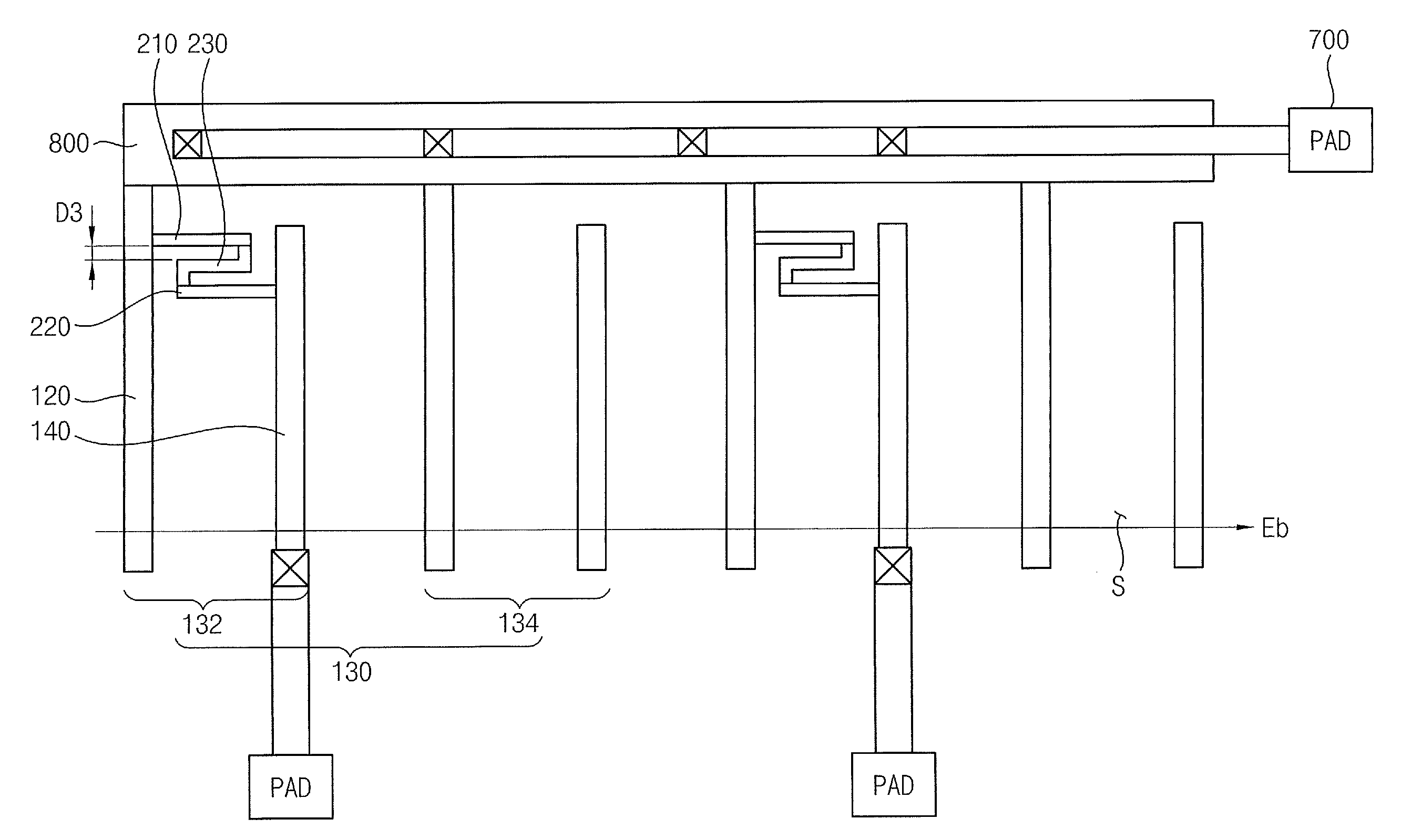
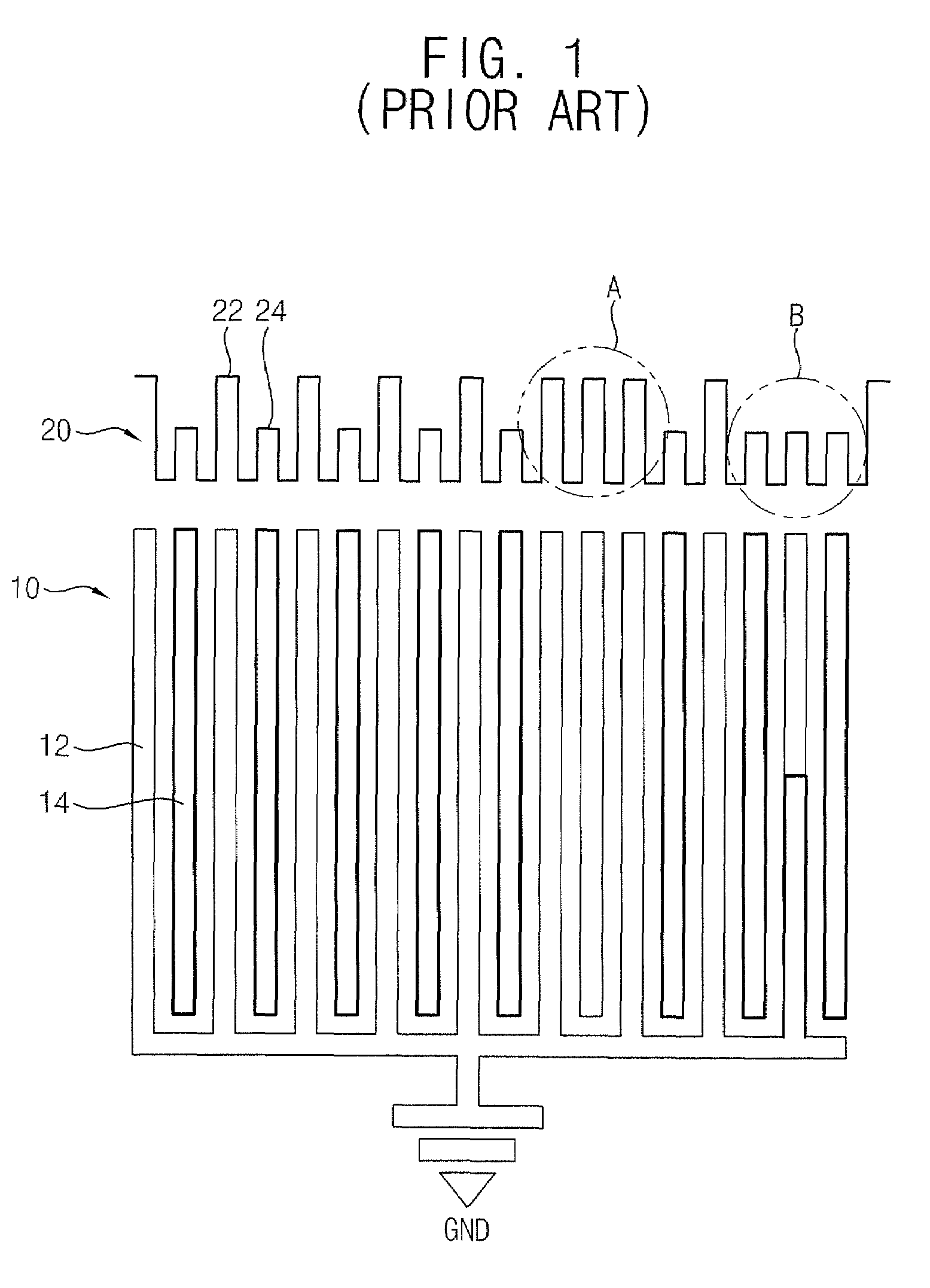
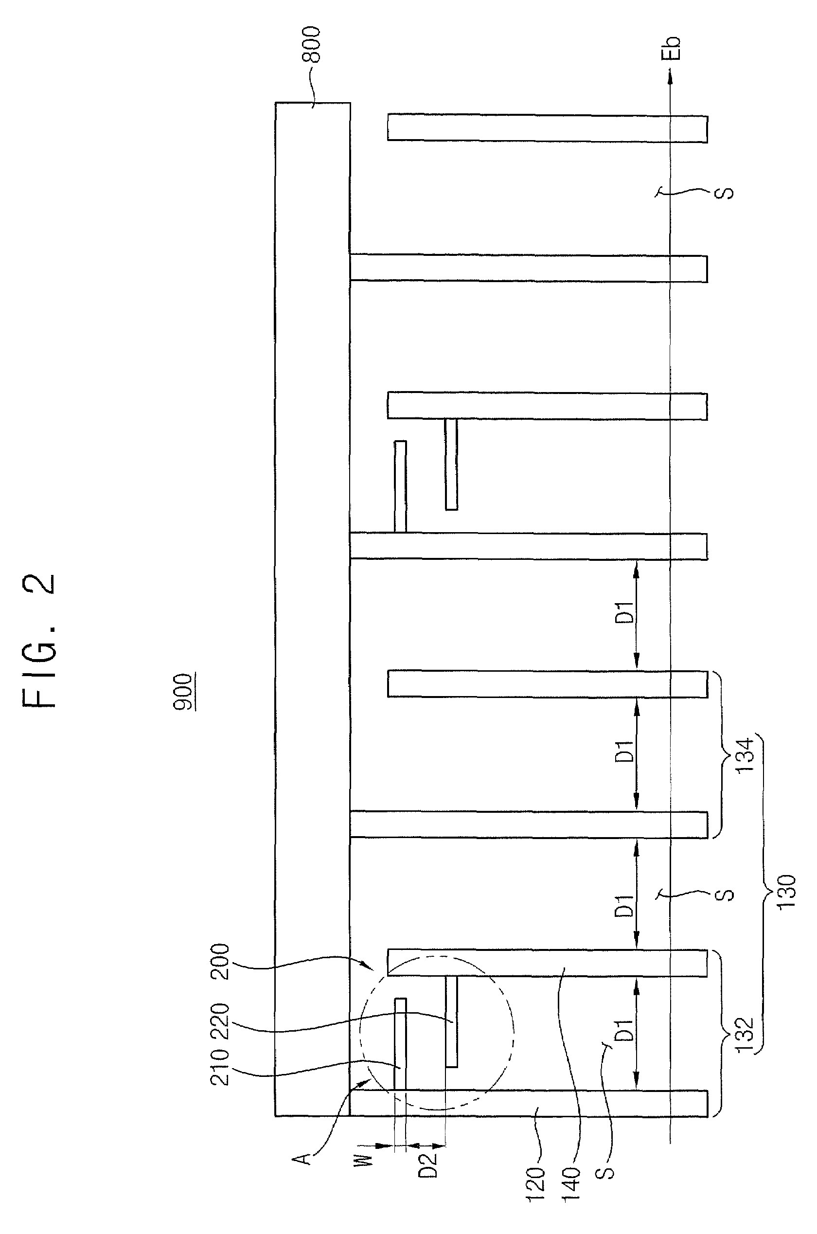
[0065]Embodiments of the invention now will be described more fully hereinafter with reference to the accompanying drawings, in which embodiments of the invention are shown. This invention may, however, be embodied in many different forms and should not be construed as limited to the embodiments set forth herein. Rather, these embodiments are provided so that this disclosure will be thorough and complete, and will fully convey the scope of the invention to those skilled in the art. Like reference numerals refer to like elements throughout.

[0066]It will be understood that when an element is referred to as being “on” another element, it can be directly on the other element or intervening elements may be present. In contrast, when an element is referred to as being “directly on” another element, there are no intervening elements present. As used herein, the term “and / or” includes any and all combinations of one or more of the associated listed items.

[0067]It will be understood that, al...


PUM


Abstract

A test structure for inspecting an allowable process margin in a manufacturing process for a semiconductor device is provided. The test structure includes a plurality of grounded conductive lines on a substrate and electrically grounded to the substrate. A plurality of floating conductive lines are provided, each of the plurality of conductive lines being spaced apart from the grounded conductive lines and electrically separated from the grounded conductive lines on the substrate. A plurality of supplementary patterns are provided for measuring the allowable process margin by a voltage contrast between the grounded conductive lines and the floating conductive lines. Related methods of testing are also provided.

Description

CLAIM OF PRIORITY[0001]This application claims priority under 35 U.S.C. § 119 to Korean Patent Application No. 2007-23809, filed on Mar. 12, 2007 in the Korean Intellectual Property Office (KIPO), the contents of which are herein incorporated by reference in their entirety.FIELD OF THE INVENTION[0002]The present invention relates generally to semiconductor devices and, more particularly to, test structures for semiconductor devices and related methods of testing.BACKGROUND OF THE INVENTION[0003]As semiconductor devices are becoming more highly integrated, design specifications for the devices, such as design rule, critical dimensions (CD) and contact area, are becoming gradually reduced. For this reason, electronic circuits on substrates are becoming more and more complicated, and circuit-packing densities for the substrates are gradually increasing. High circuit packing density requires high operation precision in each unit process for manufacturing the semiconductor devices, and t...

Claims


Application Information

Patent Timeline
Patent Type & Authority Patents(United States)
IPC IPC(8): H01L21/66
CPCH01L22/34H01L22/00
Inventor BAE, CHOEL-HWYIJIN, YOU-SEUNG
Owner SAMSUNG ELECTRONICS CO LTD
Why Eureka
Try Eureka