
Method to detect and predict metal silicide defects in a microelectronic device during the manufacture of an integrated circuit

a microelectronic device and integrated circuit technology, applied in the direction of individual semiconductor device testing, semiconductor/solid-state device testing/measurement, instruments, etc., can solve the problems of large leakage current, and inability to meet the requirements of the manufacturing process

Active Publication Date: 2008-10-28
TEXAS INSTR INC
View PDF3 Cites 70 Cited by
  • Summary
  • Abstract
  • Description
  • Claims
  • Application Information

AI Technical Summary

Benefits of technology

This approach allows for early detection of potential defects, reducing resource expenditure and improving manufacturing efficiency by predicting and correcting problematic processes, thereby enhancing the production of functional microelectronic devices.

Problems solved by technology

Unfortunately, a number of problems have been encountered when manufacturing devices having metal silicide electrodes.
In some cases, unacceptable numbers of nonfunctional transistors are constructed because of the presence of a gross short circuit caused by silicide defects.
In other instances, silicide defects from the source and drain regions punch through the source / drain junction into the semiconductor substrate, resulting in a large leakage current.
In still other cases, there is a large diode leakage between the source and drain regions and the semiconductor substrate.
These problems contribute to the production of unacceptably low yields of transistors that operate within performance specifications.
The metal silicide defects detected by this approach, however, are limited to gross shorts manifesting, for example, as metal silicide pipes in semiconductor devices.

Method used


Image

  • Method to detect and predict metal silicide defects in a microelectronic device during the manufacture of an integrated circuit
  • Method to detect and predict metal silicide defects in a microelectronic device during the manufacture of an integrated circuit
  • Method to detect and predict metal silicide defects in a microelectronic device during the manufacture of an integrated circuit

Examples


Embodiment Construction

[0014]The present invention benefits from the realization that previous approaches using passive voltage contrast imaging to detect silicide defects are inadequate because they do not predict additional silicide defects that can form after FEOL processing. Metal silicide defects are formed due to the diffusion of metal ions from metal silicide electrodes into channels in the lattice structure of the semiconductor substrate, thereby introducing structural defects in the semiconductor substrate. Defect formation is enhanced by both FEOL and BEOL thermal processing because increased temperatures promote metal ion diffusion.

[0015]As part of the present invention, it was recognized that there could be silicide defects that are too small to form a short after FEOL thermal processing and therefore go undetected using conventional approaches. In some process flows, however, a considerable number of these small silicide defects can go on to develop into shorts after BEOL thermal processing.

[...


PUM


Abstract

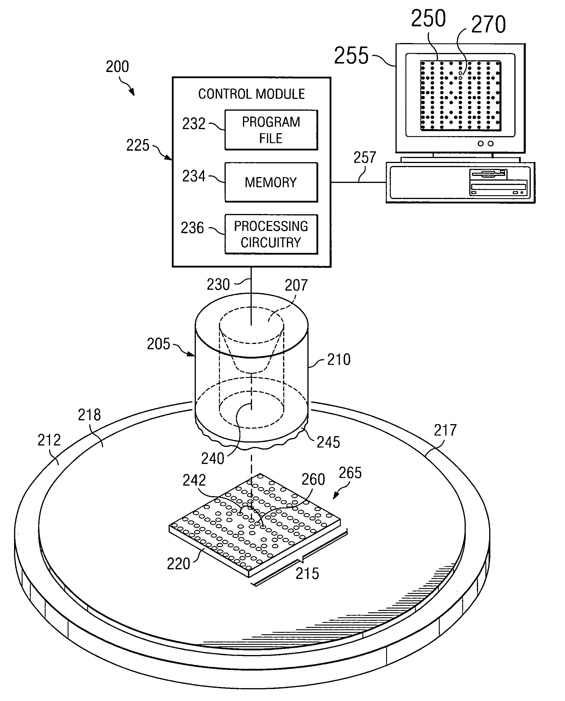
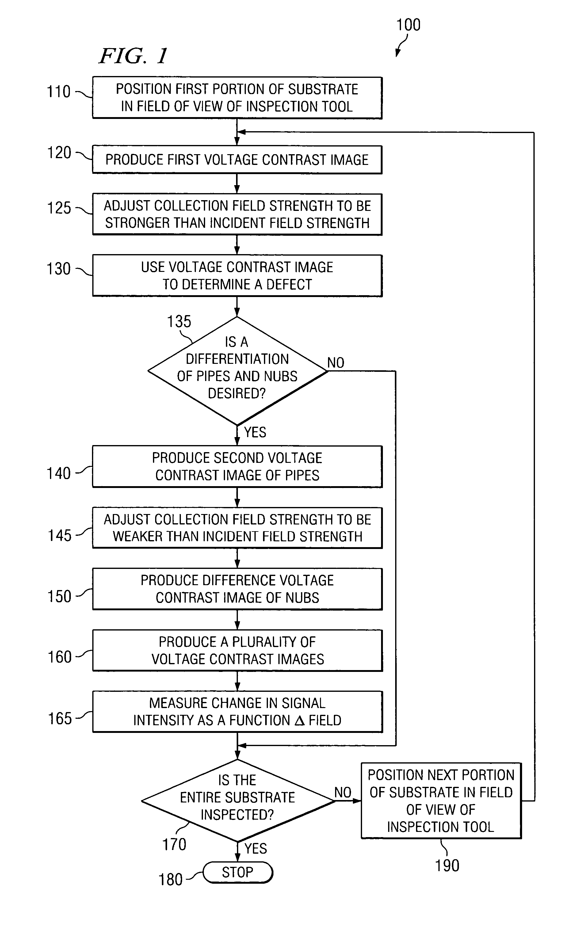
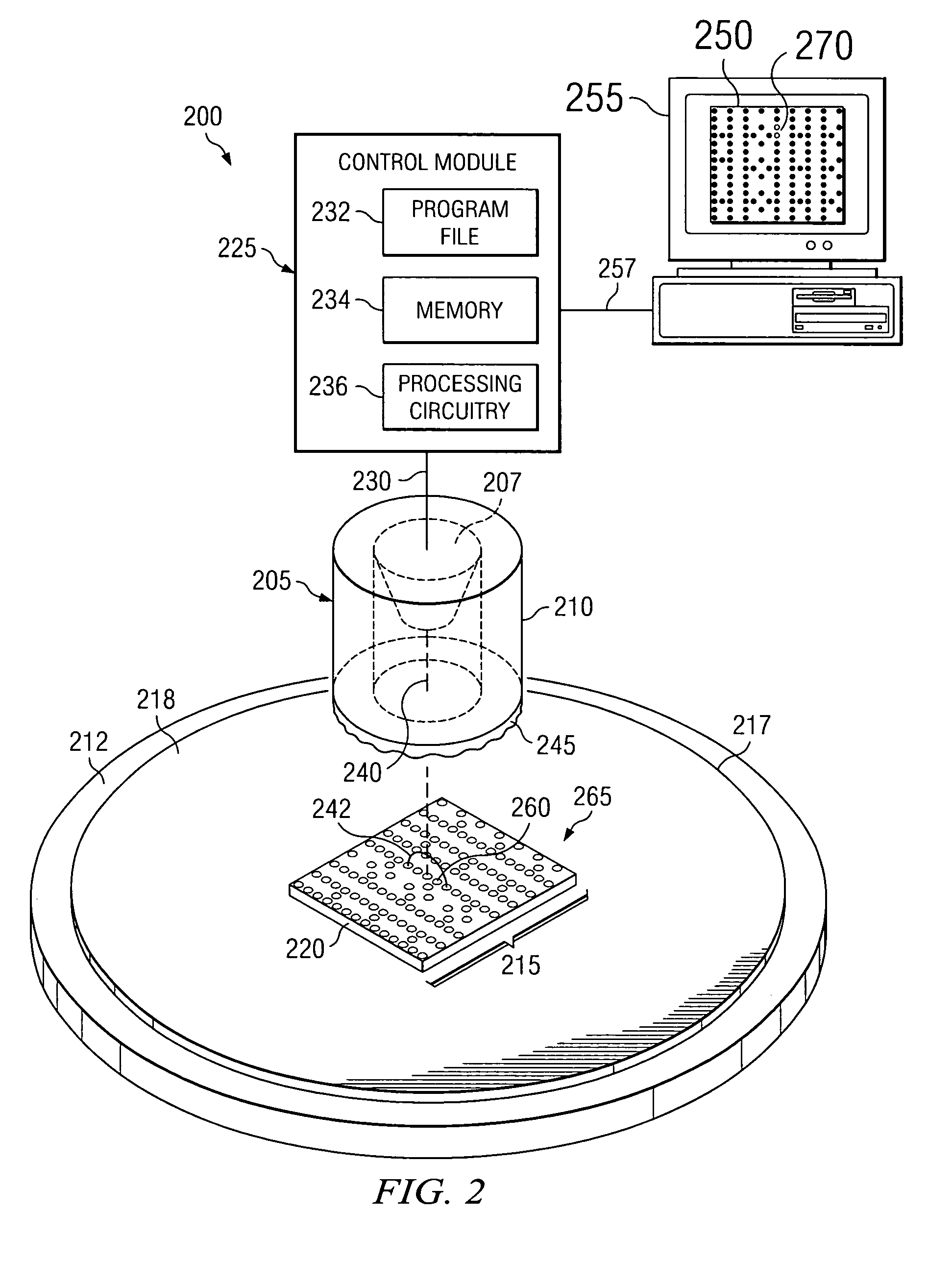
The present teachings provide methods for detection of metal silicide defects in a microelectronic device. In an exemplary embodiment, a portion of a semiconductor substrate may be positioned in a field of view of an inspection tool. The method also includes producing (120) a voltage contrast image of the portion, wherein the image is obtained using a collection field that is stronger than an incident field. The method also includes using (130) the voltage contrast image to determine a metal silicide defect in a microelectronic device. Other embodiments include an inspection system (200) for detecting metal silicide defects and a method of manufacturing an integrated circuit (300).

Description

TECHNICAL FIELD OF THE INVENTION[0001]The present invention is directed, in general, to a method and system for detecting metal silicide defects in microelectronic devices during the manufacture of integrated circuits.BACKGROUND OF THE INVENTION[0002]Metal silicides are commonly used as contact materials for active areas of microelectronic devices, such as transistors having source and drain regions and gate regions. Unfortunately, a number of problems have been encountered when manufacturing devices having metal silicide electrodes. In some cases, unacceptable numbers of nonfunctional transistors are constructed because of the presence of a gross short circuit caused by silicide defects. In other instances, silicide defects from the source and drain regions punch through the source / drain junction into the semiconductor substrate, resulting in a large leakage current. In still other cases, there is a large diode leakage between the source and drain regions and the semiconductor subs...

Claims


Application Information

Patent Timeline
Patent Type & Authority Patents(United States)
IPC IPC(8): G01R31/06
CPCG01R31/307
Inventor RAMAPPA, DEEPAK A.
Owner TEXAS INSTR INC
Learn More