Method of manufacturing wiring board

a manufacturing method and technology of wiring boards, applied in the field of manufacturing wiring boards, can solve the problems of large distortion in the resin layer, excessive thick product, and inability to meet the recent demand for a reduction in the thickness of wiring boards, so as to improve the productivity and reliability of wiring boards, and the effect of easy separation from the adhesive layer

Active Publication Date: 2012-11-06
TDK CORPARATION
View PDF21 Cites 2 Cited by
  • Summary
  • Abstract
  • Description
  • Claims
  • Application Information

AI Technical Summary

Benefits of technology

[0009]The present invention has been made in light of the above circumstances, and therefore has an object to provide a method of manufacturing a wiring board with which: when forming a multilayer wiring structure by a build-up process or the like, distortion and deformation of the wiring board, which might be caused during manufacturing, are sufficiently prevented, and also an adhesive, etc., are prevented from adhering to the multilayer wiring structure formed on a support substrate, thereby reducing the effect on the subsequent manufacturing process, leading to improved productivity; and recycling of the support substrate is attained.
[0011]In the wiring board manufacturing method with the above structure, the second composite body is attached to the support substrate through the first composite body, forming an integrated body, and the stacked layers structure obtained by laminating the conductive layer and the resin insulating layer is formed on the integrated body. Accordingly, dimensional changes, distortion, deformation, etc., of the stacked layers structure, which might be caused due to rigidity and tenacity of the support substrate during manufacturing, are prevented.
[0012]After forming the stacked layers structure on the second composite body, the thermally foamable adhesive layer in the first composite body is heated, whereby the thermal foaming agent contained in that layer is thermally decomposed to generate gas, and that gas breaks through the thermally foamable adhesive layer to be released to the outside. As a result, the adhesion area between the thermally foamable adhesive layer and the support substrate is reduced. Therefore, the support substrate and the first composite body are separated from each other at the adhesion boundary therebetween; alternatively, both become easily separable, and so are mechanically peeled from each other for the separation. Accordingly, an adhesive component in the thermally foamable adhesive layer becomes difficult to adhere to the support substrate, which eliminates the troublesome process involved with removing the adhesive component from the support substrate, enabling simple recycling of the support substrate.
[0013]Moreover, after performing the separation of the support substrate, the carrier foil layer is peeled from the carrier-foil coated metal foil, whereby the bonded body constituted by the metal foil layer and the stacked layers structure is separated from the bonded body constituted by the carrier foil layer and the first composite body. As a result, the adhesive component in the adhesive layer does not adhere to the bonded body constituted by the metal foil layer and the stacked layers structure (i.e., the wiring board), and outer layer wiring can be formed reliably and simply in the metal foil layer. Accordingly, productivity and reliability of the wiring board can be improved. Furthermore, the carrier-foil coated metal foil is formed by bonding the metal foil layer and the carrier foil layer, which are formed as separate members, and therefore, the metal foil layer is easily formable with a small and uniform thickness. Accordingly, the minute outer layer wiring can be formed in the metal foil layer.
[0016]More specifically, a structure in which the first composite body has a base provided between a thermally foamable adhesive layer and an adhesive layer can be given as an example. This structure has the advantage that the thermally foamable adhesive layer can be separated from the adhesive layer more easily.
[0017]According to the invention, a second composite body is attached to a support substrate through a first composite body, forming an integrated body; a stacked layers structure obtained by laminating a conductive layer and a resin insulating layer is formed thereon; thereafter, separation of the support substrate is performed; and further, separation for removal of a carrier foil layer in the second composite body is performed, whereby a wiring board having a metal foil layer and the stacked layers structure is obtained. Accordingly, dimensional changes, distortion, deformation, etc., of the wiring board, which might be caused during manufacturing, can be sufficiently prevented, and also an adhesive, etc., are prevented from adhering to the stacked layers structure formed on the support substrate, thereby reducing the effect on the subsequent manufacturing process, leading to improved productivity and reliability of the wiring board. Also, recycling of the support substrate can be performed reliably and simply.

Problems solved by technology

However, when using the above core layer, a wiring board that is the final product becomes excessively thick, and this may not satisfy the recent demand for a reduction in thickness of wiring boards.
However, this method causes a large distortion in the resin layers due to the influence of heat applied during manufacturing and moisture.
This will cause connection failures when an electrode pitch of, e.g., a semiconductor IC built into a wiring board is narrow.
However, the above wiring board tends to have a structural defect such as a warp or a crack during handling.
However, in the current manufacturing of a multilayer wiring board by a build-up process, there is a tendency for overlaying a large number of extremely thin resin layers.
According to the inventor's finding, it has been found that performing heat treatment and pressure treatment many times on a support substrate leads to noticeable deterioration of an adhesive or adhesive agent layer (resin) that supports the support substrate in a fixed manner.
For example, in the method disclosed in JP2007-173622 A, there is concern that a part of the deteriorated adhesive agent layer adheres to the stacked layers structure separated from the support substrate, and if this state remains, it becomes difficult for the subsequent wiring process, etc., to be performed.
The residue of the sheet base adheres to the stacked layers structure, and thus becomes difficult to be removed, which negatively affects the subsequent wiring process, etc.
Moreover, the sheet base and the adhesion layer which adhere to the base dielectric layer remain on the support substrate, and this makes the support substrate difficult to be recycled (reused).

Method used


Image

  • Method of manufacturing wiring board
  • Method of manufacturing wiring board
  • Method of manufacturing wiring board

Examples


Embodiment Construction

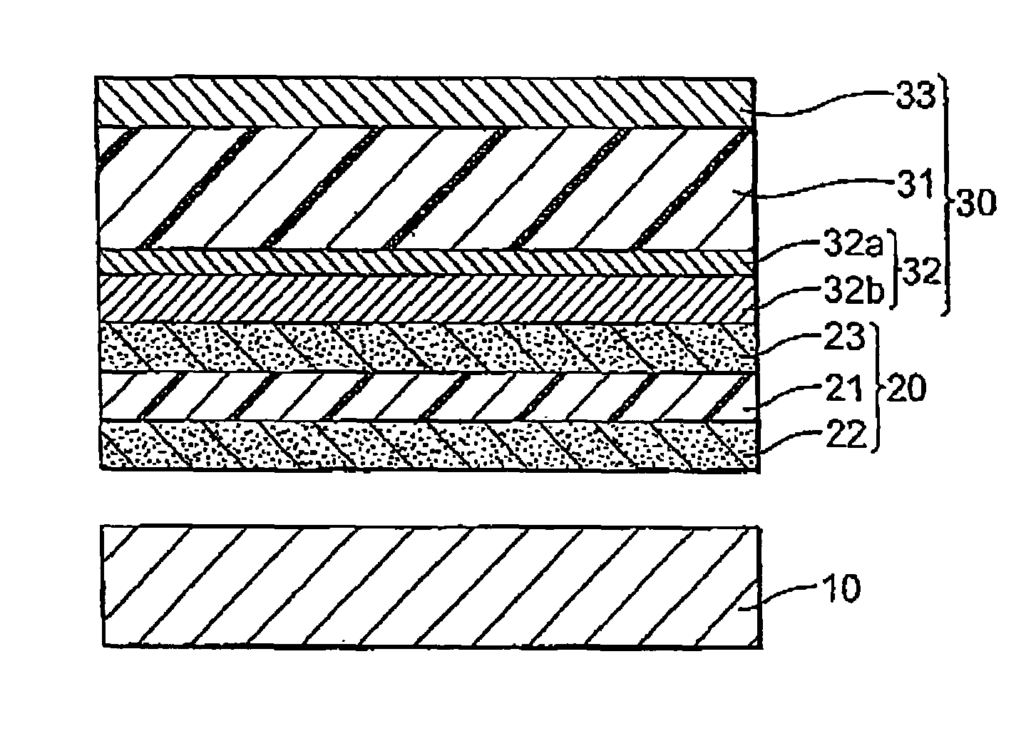
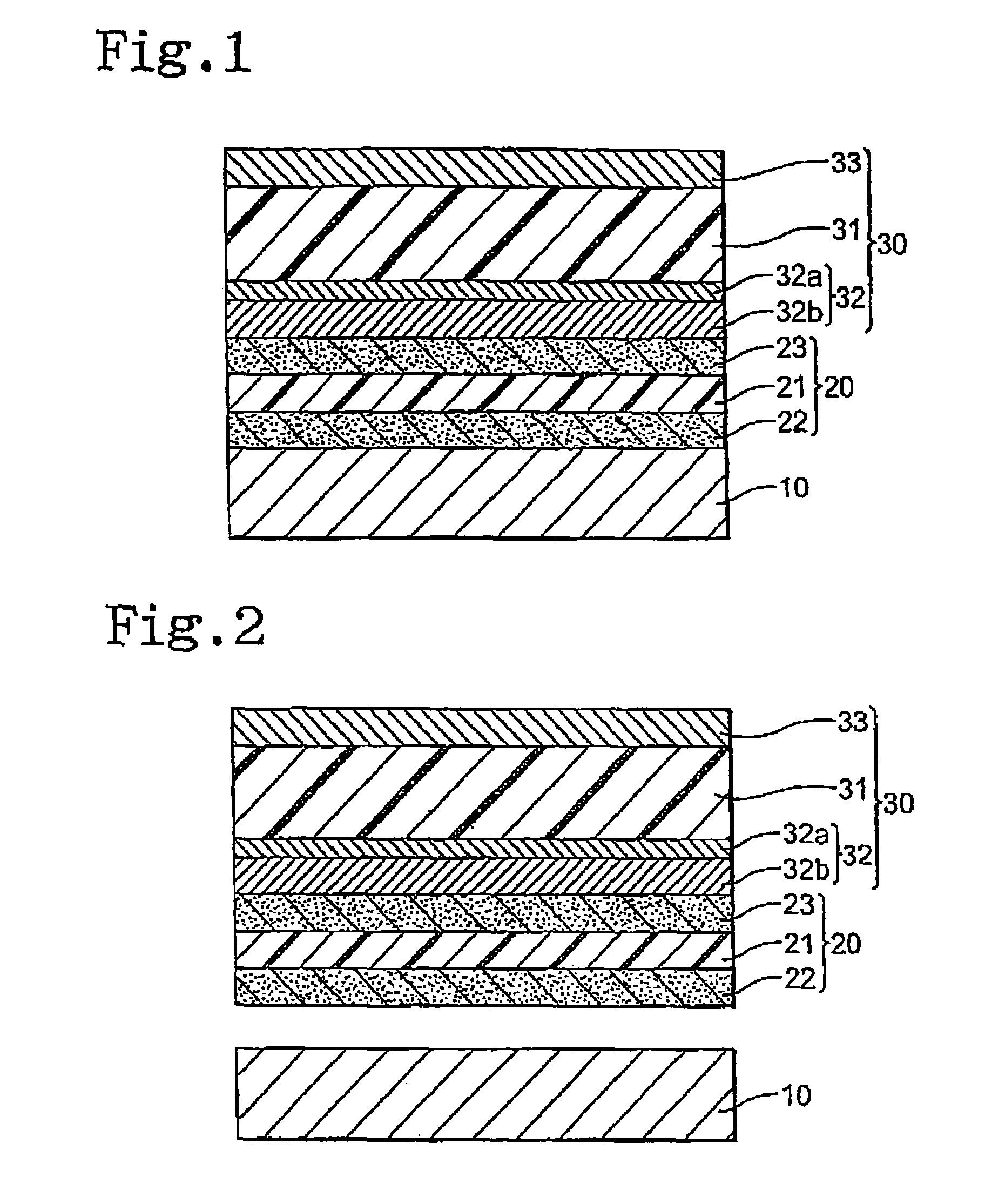
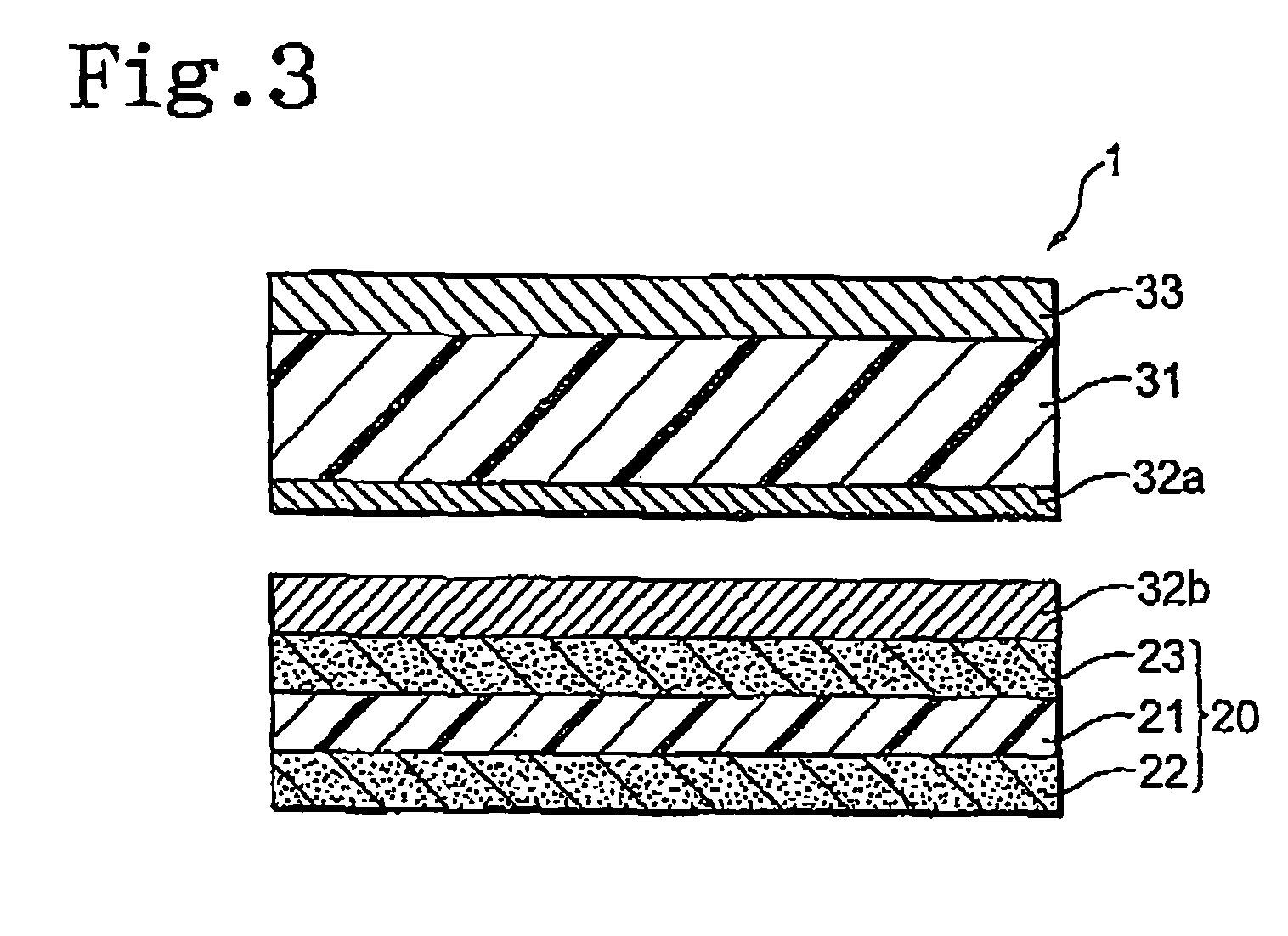
[0021]An embodiment of the invention will hereinafter be described in detail. Note that like components are denoted by like reference symbols and will not be further explained. It is assumed that vertical and horizontal positional relations are based on the positional relations shown in the drawings, unless otherwise specified. Also, a dimensional ratio of the drawings is not limited to a shown ratio. Moreover, the following embodiment is for explaining the invention, and is not intended to limit the invention to the embodiment only. Furthermore, various modifications of the invention may be made without departing from the gist of the invention.

[0022]FIGS. 1 to 3 each are a process drawing showing a state of manufacturing of a wiring board in accordance with an embodiment of a method of manufacturing a wiring board according to the invention. In this embodiment, first, a support substrate 10 is prepared. Materials for the support substrate 10 are not particularly limited as long as ...


PUM

PropertyMeasurementUnit
thermally foamableaaaaaaaaaa
densityaaaaaaaaaa
dielectricaaaaaaaaaa

Abstract

Provided is a method of manufacturing a wiring board, in which: a composite adhesive sheet 20 is attached to one of the surfaces of a support substrate 10, and a double-sided CCL 30 is attached to the other surface. Then, in an integrated state of the above components, a multilayer wiring structure including a conductive layer and a resin insulating layer is formed on a metal layer 33 of the double-sided CCL 30 by a known build-up method. A thermally foamable adhesive layer 22 of the composite adhesive sheet 20 is then heated, thereby thermally decomposing a thermal foaming agent to generate gas, and the support substrate 10 is separated from the remaining bonded body. Thereafter, a carrier foil layer 32b and a copper foil layer 32a of a carrier-foil coated copper foil 32 are mechanically peeled from each other at a boundary between both the layers, thereby obtaining a wiring board 1.

Description

CROSS-REFERENCES TO RELATED APPLICATIONS[0001]The entire disclosure of Japanese Patent Application No. 2008-220961, filed on Aug. 29, 2008, is expressly incorporated herein by reference.BACKGROUND[0002]1. Technical Field[0003]The present invention relates to a method of manufacturing a wiring board (substrate).[0004]2. Related Art[0005]In recent years, there has been more demand than ever before for the demand for electronic equipment including portable equipment typified by, e.g., mobile telephones to be provided in higher-density packaging. In order to respond to this demand, higher-density wiring and an increase in the number of terminals have been eagerly sought for substrate modules and wiring boards which are provided with electronic components. Examples of such wiring boards include various kinds of build-up multilayer wiring boards such as one having, on an insulating core layer, a stacked layers structure obtained by alternately laminating insulating layers or dielectric la...

Claims


Application Information

Patent Timeline
Patent Type & Authority Patents(United States)
IPC IPC(8): B32B38/10
CPCH05K3/007H05K3/025H05K3/4602H05K3/4682B32B43/006B32B37/12Y10T156/11B32B2038/0084B32B2457/08H05K3/386H05K2203/0152H05K2203/0156H05K2203/0191H05K2203/0264H05K2203/1105Y10T29/49117Y10T29/49126Y10T156/1142Y10T29/49124
Inventor KAWABATA, KENICHIOHKAWA, HIROSHIGE
Owner TDK CORPARATION
Why Eureka
Try Eureka