Plasma processing apparatus and plasma etching method

a technology of plasma processing and plasma, applied in the field of technology, can solve the problems of deterioration of uniformity, difficulty in implementing a chamber structure, and increase production yield, and achieve the effects of improving the uniformity of cd, reducing the difficulty of etching, and effectively altering the etching rate at the substrate edge portion

Active Publication Date: 2012-11-06
TOKYO ELECTRON LTD
View PDF9 Cites 4 Cited by
  • Summary
  • Abstract
  • Description
  • Claims
  • Application Information

AI Technical Summary

Benefits of technology

[0008]In view of the above, the present invention provides a capacitively coupled plasma processing apparatus capable of controlling a distribution characteristic of an electron density or process characteristics on a substrate to be processed easily and arbitrarily.
[0009]The present invention also provides a plasma etching method capable of improving uniformity of etching characteristics in various etching processes.

Problems solved by technology

In the capacitively coupled plasma processing apparatus which realize the plasma having the large diameter, however, it has been difficult to carry out the plasma process uniformly on every position on the substrate, and this problem has been an obstacle to the enhancement of production yield.
Thus, although a highly uniform process result is obtained under a certain processing condition, the uniformity may be deteriorated if a processing condition is changed to obtain required processing characteristics.
In fact, it is difficult to implement a chamber structure which guarantees high process uniformity under a wide range of processing conditions.
Especially, in case of etching multilayer films on a substrate in plural steps consecutively, it is difficult to obtain the process uniformity with fine etching characteristics in every step because process parameters or materials of etching masks employed in each step or for each film to be processed are different.
Thus, it has been difficult to be dealt with various processes or variations in processing conditions flexibly, so that recently required high level of plasma process uniformity could not be achieved.

Method used


Image

  • Plasma processing apparatus and plasma etching method
  • Plasma processing apparatus and plasma etching method
  • Plasma processing apparatus and plasma etching method

Examples


Embodiment Construction

[0038]Hereinafter, embodiments of the present invention will be described with reference to the accompanying drawings which form a part hereof.

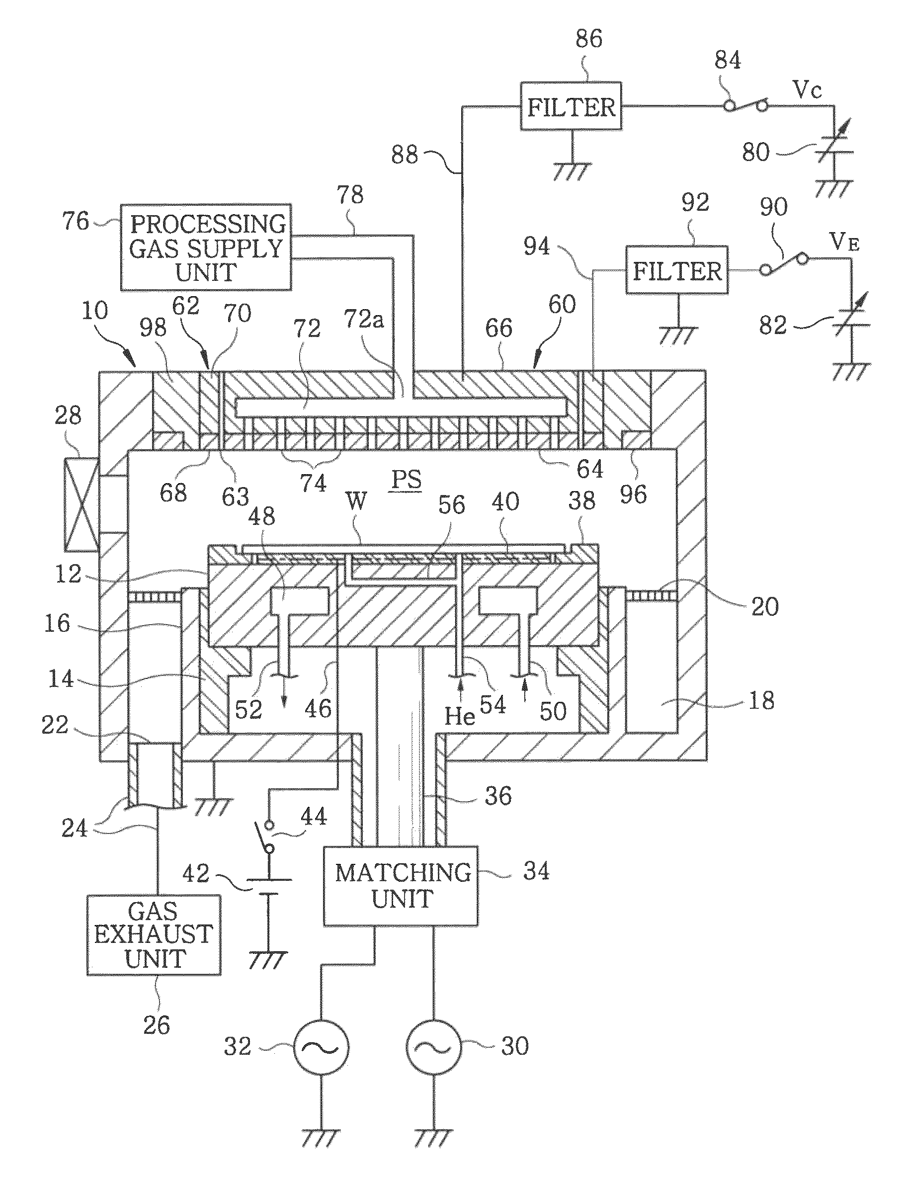
[0039]FIG. 1 illustrates a configuration of a plasma etching apparatus in accordance with an embodiment of the present invention. The plasma etching apparatus is configured as a capacitively coupled plasma etching apparatus of a cathode coupling type employing a lower electrode dual frequency application type. The plasma etching apparatus includes a cylindrical chamber (processing chamber) 10 made of a metal such as aluminum, stainless steel, or the like. The chamber 10 is frame-grounded.

[0040]A circular plate-shaped susceptor 12 serving as a lower electrode for mounting thereon a substrate to be processed, e.g., a semiconductor wafer W, is disposed horizontally in the chamber 10. The susceptor 12 is made of, e.g., aluminum, and is supported by a cylindrical insulating support 14 extending vertically upward from a bottom of the chamber 10.

[00...


PUM

PropertyMeasurementUnit
voltageaaaaaaaaaa
DC voltageaaaaaaaaaa

Abstract

A plasma processing apparatus includes an inner upper electrode provided to face a lower electrode mounting thereon a substrate, an outer upper electrode provided in a ring shape at a radially outside of the inner upper electrode and electrically isolated from the inner upper electrode in a vacuum evacuable processing chamber and a processing gas supply unit for supplying a processing gas into a processing space between the inner and the outer upper electrode and the lower electrode. A radio frequency (RF) power supply unit is also provide to apply a RF power to the lower electrode or the inner and the outer upper electrode to generate a plasma of the processing gas by RF discharge. A first and a second DC power supply unit are provided to apply a first and a second variable DC voltage to the inner upper electrode, respectively.

Description

FIELD OF THE INVENTION[0001]The present invention relates to a technique for performing a plasma process on a substrate to be processed; and, more particularly, to a capacitively coupled plasma processing apparatus and a plasma etching method using same.BACKGROUND OF THE INVENTION[0002]In a manufacturing process of a semiconductor device or an FPD (Flat Panel Display), a plasma is often used in the process, e.g., etching, deposition, oxidation, sputtering or the like, in order to allow a processing gas to react efficiently at a relatively low temperature. Conventionally, a capacitively coupled plasma processing apparatus is mainly used to easily realize a plasma having a large diameter for single-wafer plasma processing apparatuses.[0003]In general, the capacitively coupled plasma etching apparatus has a configuration in which an upper electrode and a lower electrode are disposed in parallel to each other in a vacuum processing chamber. A substrate to be processed (a semiconductor w...

Claims


Application Information

Patent Timeline
Patent Type & Authority Patents(United States)
IPC IPC(8): B44C1/22C03C15/00C03C25/68C23F1/00
CPCH01J37/32027H01J37/32091
Inventor HONDA, MASANOBUMASUZAWA, KENJINAKAYAMA, HIROYUKIIWATA, MANABUSATO, MANABUNARISHIGE, KAZUKI
Owner TOKYO ELECTRON LTD
Why Eureka
Try Eureka