
Method for manufacturing a heat dissipation structure of a printed circuit board

a technology of printed circuit board and heat dissipation structure, which is applied in the manufacture of cable/conductor, printed electric component incorporation, conductive pattern formation, etc., can solve the problems of variation of resistance value, difficult control of polishing process, and difficult to fully fill opening, so as to achieve easy control of resistance value of plated copper layer

Active Publication Date: 2012-11-20
KINSUS INTERCONNECT TECH
View PDF6 Cites 0 Cited by
  • Summary
  • Abstract
  • Description
  • Claims
  • Application Information

AI Technical Summary

Benefits of technology

[0009]In the present invention, when the substrate has the openings with different sizes and the copper cannot be plated in the openings once, the nickel plating layer is formed as a barrier layer to avoid the uneven surface caused by performing the copper plating process for many times. Furthermore, by sandwiching the nickel plating layer between the copper plating layers, the resistance value of the plated copper layer can be easily controlled, and thereby the problems in the prior art can be solved.

Problems solved by technology

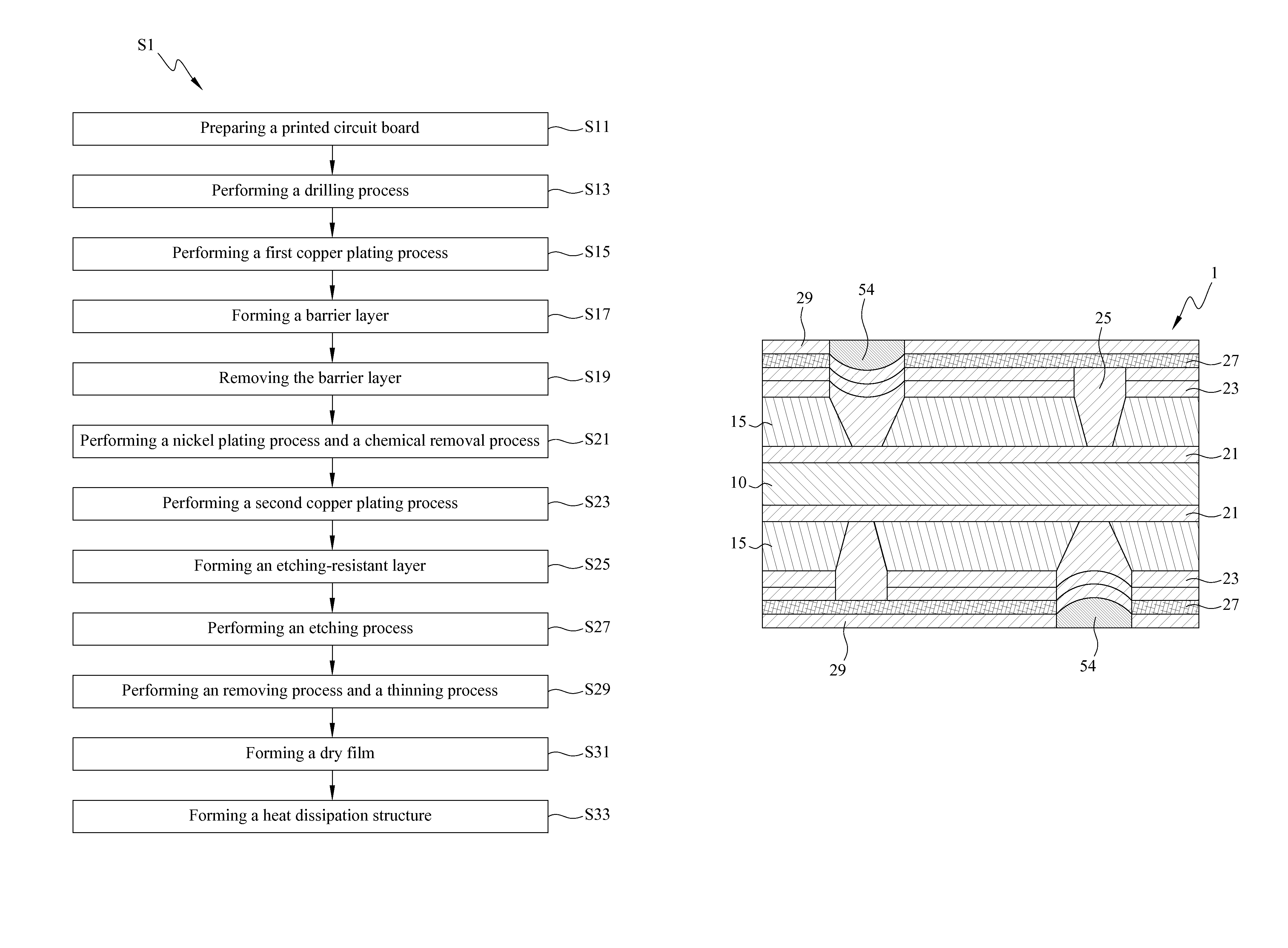
In the prior art, because the size of the opening is larger than or equal to the size of 150×100 μm2, the opening is not easily to be fully filled up by performing the copper plating process only once, and thereby the copper plating process must be performed for many times in order to fill up the opening.
However, there exists an uneven surface problem caused by the interface between the two adjacent copper plating layers when the copper plating process is performed for many times, which results in the variation of the resistance values.
Therefore, a polishing process is needed in order to meet the specification of the resistance value, but the polishing process is not easily controlled so that the resistance value cannot be standarized.

Method used


Image

  • Method for manufacturing a heat dissipation structure of a printed circuit board
  • Method for manufacturing a heat dissipation structure of a printed circuit board
  • Method for manufacturing a heat dissipation structure of a printed circuit board

Examples


Embodiment Construction

[0014]The accompanying drawings are included to provide a further understanding of the invention, and are incorporated in and constituted a part of this specification. The drawings illustrate an embodiment of the invention and, together with the description, serve to explain the principles of the invention.

[0015]FIG. 2 is a flowchart showing the steps of the method for manufacturing a heat dissipation structure of a printed circuit board according to the present invention. FIGS. 3A to 3L are cross-sectional views illustrating the steps of the method for manufacturing a heat dissipation structure of a printed circuit board according to one embodiment of the present invention. Referring to FIG. 2, the method for manufacturing the heat dissipation structure of the printed circuit board of the present invention (S1) comprises: a step of preparing a printed circuit board (S11), a step of performing a drilling process (S13), a step of performing a first copper plating process (S15), a ste...


PUM

PropertyMeasurementUnit
sizeaaaaaaaaaa
heightaaaaaaaaaa
thicknessaaaaaaaaaa

Abstract

A method for manufacturing a heat dissipation structure of a printed circuit board includes: forming a barrier layer on the dimple in the first copper plating layer; forming a nickel plating layer; removing the nickel plating layer and the barrier layer on the dimple; forming a second copper plating layer to make the total height of the first copper plating layer and the second copper plating layer in the second opening higher than that of the first copper plating layer in the first opening; filling the dimple in the second copper plating layer with an etching-resistant material; removing the second copper plating layer; removing the nickel plating layer and the etching-resistant material to make the second copper plating layer in the second opening being at the same height as the first copper plating layer in the first opening; and forming the heat dissipation structure by photolithography.

Description

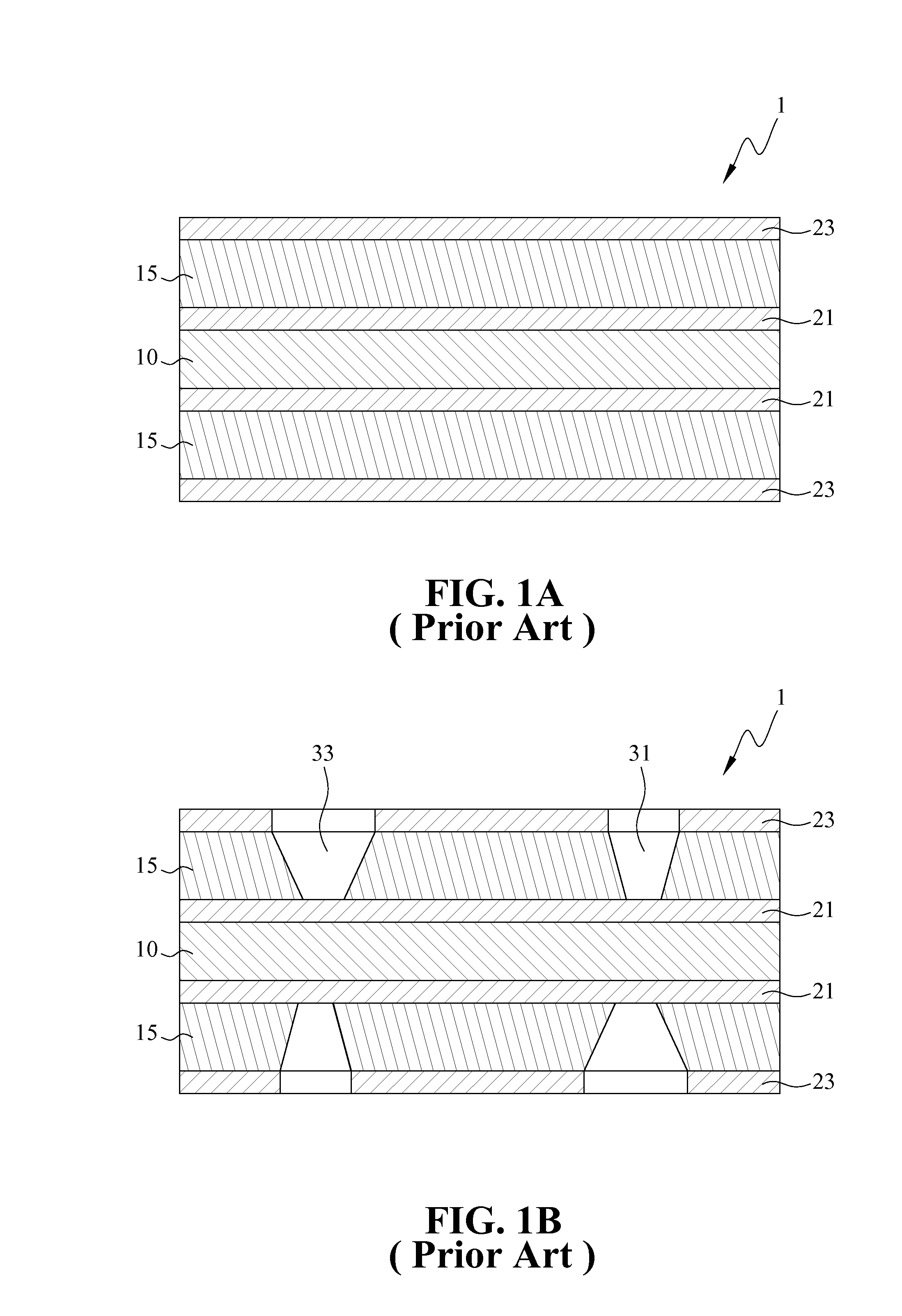
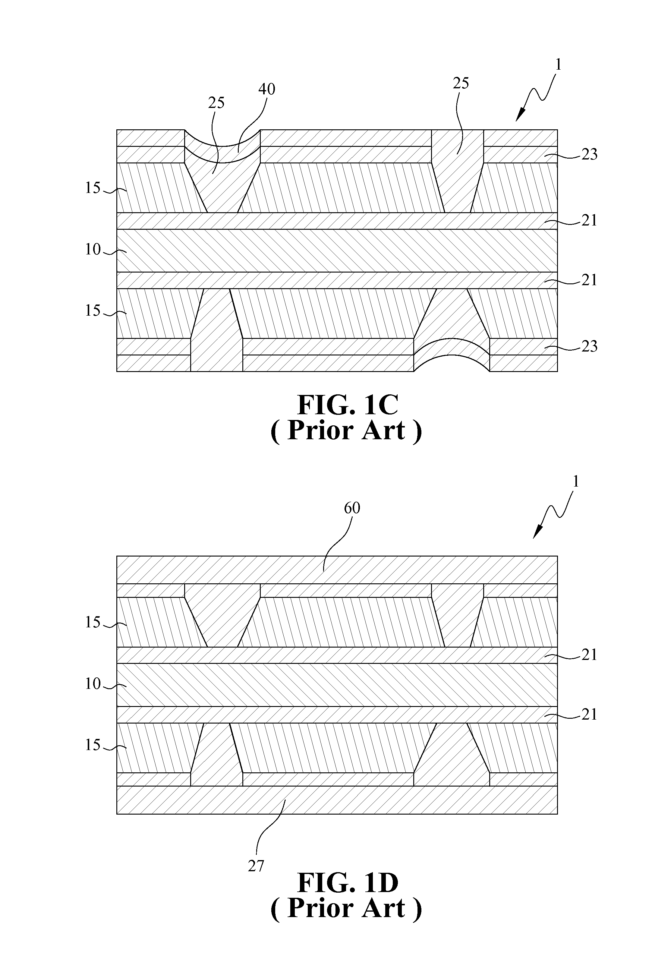
BACKGROUND OF THE INVENTION[0001]1. Field of the Invention[0002]The present invention relates to a method for manufacturing a heat dissipation structure of a printed circuit board, and more particularly to a method for manufacturing a heat dissipation structure of a printed circuit board for improving the filling capability of plating copper, and improving the uneven surface caused by performing the copper plating process for many times using a nickel plating process.[0003]2. The Prior Arts[0004]FIGS. 1A to 1F are cross-sectional views illustrating the steps of a conventional method for manufacturing a heat dissipation structure of a printed circuit board. Referring to FIG. 1A, a printed circuit board 1 is provided. The printed circuit board 1 includes a first substrate 10, two second substrates 15 respectively disposed on the upper and lower surfaces of the first substrate 10, two inner copper layers 21 each disposed between the first substrate 10 and the second substrate 15, and t...

Claims


Application Information

Patent Timeline
Patent Type & Authority Patents(United States)
IPC IPC(8): H05K3/02
CPCH05K3/421H05K3/427H05K1/0206Y10T29/49155H05K2203/0733Y10T29/49156Y10T29/49165H05K2203/025
Inventor CHANG, CHIEN-WEILIN, TING-HAOCHEN, YA-HSIANGLU, DE-HAO
Owner KINSUS INTERCONNECT TECH
Learn More